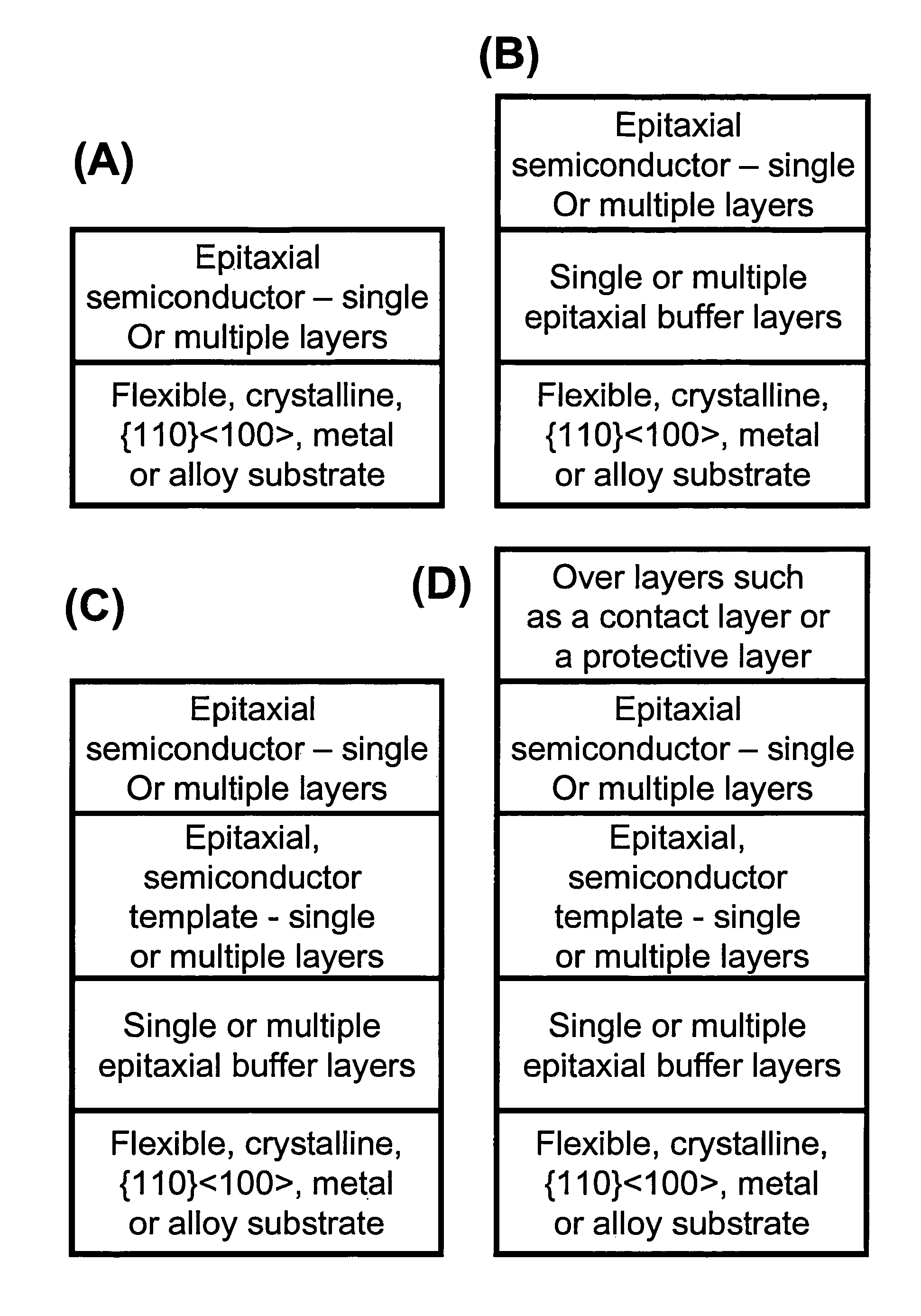
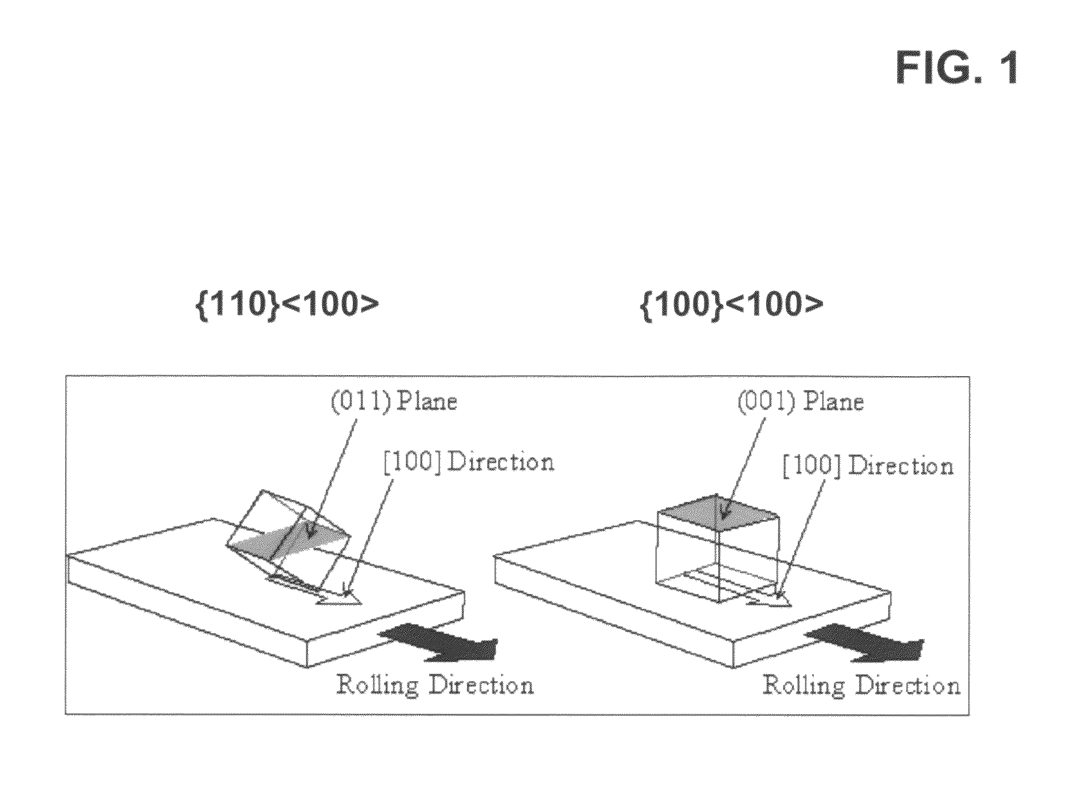
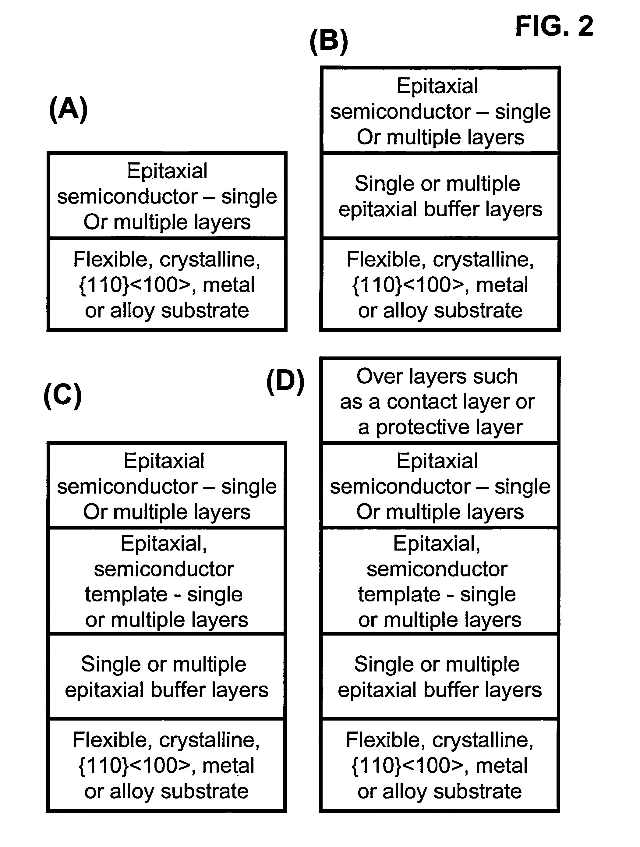
Semiconductor-based, large-area, flexible, electronic devices on {110}<100> oriented substrates

a technology of semiconductors and substrates, applied in the direction of final product manufacturing, semiconductor/solid-state device details, sustainable manufacturing/processing, etc., can solve the problems of unrealized solar energy promise, prohibitively expensive cost of single crystal substrates, unfavorable price/performance metric, etc., and achieve high performance

a technology of semiconductors and substrates, applied in the direction of final product manufacturing, semiconductor/solid-state device details, sustainable manufacturing/processing, etc., can solve the problems of unrealized solar energy promise, prohibitively expensive cost of single crystal substrates, unfavorable price/performance metric, etc., and achieve high performance

US8795854B2Inactive Publication Date: 2014-08-05GOYAL AMIT

Image

  • Semiconductor-based, large-area, flexible, electronic devices on {110}&#x3c;100&gt; oriented substrates
  • Semiconductor-based, large-area, flexible, electronic devices on {110}&#x3c;100&gt; oriented substrates
  • Semiconductor-based, large-area, flexible, electronic devices on {110}&#x3c;100&gt; oriented substrates

Examples


example 1

[0108]Starting with a secondary recrystallized, Fe-3 at % Si substrate, with a {110} orientation, a 10-75 nm thick, epitaxial layer of TiN is grown by electron beam evaporation, sputtering, pulsed laser ablation or chemical vapor deposition at a substrate temperature in the range of 300-850° C. This is followed by deposition of an epitaxial Si layer using chemical vapor deposition in the temperature range of 300-900° C.

example 2

[0109]Starting with a secondary recrystallized, Fe-3 at % Si substrate, with a {110} orientation, a 10-75 nm thick, epitaxial layer of TiN is grown by electron beam evaporation, sputtering, pulsed laser ablation or chemical vapor deposition at a substrate temperature in the range of 300-850° C. This is followed by deposition of a 10-75 nm thick, epitaxial, layer of MgO by electron beam evaporation, sputtering, pulsed laser ablation or chemical vapor deposition at a substrate temperature in the range of 300-850° C. This is followed by deposition of an epitaxial Si layer using chemical vapor deposition in the temperature range of 300-900° C.

example 3

[0110]Starting with a secondary recrystallized, Fe-3 at % Si substrate, with a {110} orientation, a 10-75 nm thick, epitaxial layer of γ-Al2O3 is grown by electron beam evaporation, sputtering, pulsed laser ablation or chemical vapor deposition at a substrate temperature in the range of 300-850° C. This is followed by deposition of an epitaxial Si layer using chemical vapor deposition in the temperature range of 300-900° C. Numerous reports exist in the literature of epitaxial growth of Si on γ-Al2O3 (see for example, Liwen tan, Qiyuan Wang, Jun Wang, Yuanhuan Yu, Zhongli Liu and Lanying Lin, “Fabrication of novel double-hetero-epitaxial SOI structure Si / γ-Al2O3 / Si,” Journal of Crystal Growth, vol. 247, pp. 255-260, 2003; K. Sawada, M. Ishida, T. Nakamura and N. Ohtake, “Metalorganic molecular beam epitaxy of films on Si at low growth temperatures,” Appl. Phys. Lett., vol. 52, pp. 1672-1674, 1988; M. Shahjahan, Y. Koji, K. Sawada and M. Ishida, “Fabrication of resonance tunnel diode...


PUM

PropertyMeasurementUnit
grain sizeaaaaaaaaaa
rotation angleaaaaaaaaaa
diameteraaaaaaaaaa

Abstract

Novel articles and methods to fabricate the same resulting in flexible, oriented, semiconductor-based, electronic devices on {110}<100> textured substrates are disclosed. Potential applications of resulting articles are in areas of photovoltaic devices, flat-panel displays, thermophotovoltaic devices, ferroelectric devices, light emitting diode devices, computer hard disc drive devices, magnetoresistance based devices, photoluminescence based devices, non-volatile memory devices, dielectric devices, thermoelectric devices and quantum dot laser devices.

Description

CROSS-REFERENCE TO RELATED APPLICATIONS[0001]This application is (1) a continuation-in-part of U.S. patent application Ser. No. 11 / 498,120, filed Aug. 3, 2006, now U.S. Pat. No. 8,119,571, which claimed priority to U.S. provisional patent application Ser. No. 60 / 704,264, both of which are herein incorporated by reference in entirety and (2) a continuation-in-part of U.S. patent application Ser. No. 11 / 715,047, filed Mar. 8, 2007, now U.S. Pat. No. 7,906,229, which is also herein incorporated by reference in its entirety.STATEMENT REGARDING FEDERALLY FUNDED RESEARCH OR DEVELOPMENT[0002]This invention was made with Government support under Contract No. DE-AC05-000R22725 awarded by the United States Department of Energy. The Government has certain rights in this invention.FIELD OF THE INVENTION[0003]The invention relates to fabrication of high performance electronic devices comprising various types of semiconductors and articles made therefrom.BACKGROUND OF THE INVENTION[0004]Electroni...

Claims


Application Information

Patent Timeline
05 Aug 2014
Publication
US8795854B2
IPC
B32B9/00; B32B15/04; H01L29/04; H01L31/09; B82Y10/00; H01L21/02; H01L29/786; H01L31/036; H01L31/0392; H01L31/0687; H01L31/18
CPC
H01L21/02433; B82Y10/00; H01L21/02439; H01L31/0392; H01L31/1872; H01L21/02491; H01L29/78603; Y02E10/544
Inventors
GOYAL, AMIT