Photoelectric conversion element, production method thereof, photosensor, imaging device and their driving method

a technology of photoelectric conversion and production method, which is applied in the direction of sustainable manufacturing/processing, instruments, and radiation control devices, can solve the problems of reducing the aperture ratio, reducing the light collection efficiency and the resulting reduction in sensitivity, and disadvantageously increasing the dark current, so as to reduce the range of increase in the dark current and low dark current

Active Publication Date: 2014-09-30
FUJIFILM CORP
View PDF40 Cites 19 Cited by
  • Summary
  • Abstract
  • Description
  • Claims
  • Application Information

AI Technical Summary

Benefits of technology

[0058]According to the present invention, a photoelectric conversion element capable of functioning as a photoelectric conversion element when a compound having a specific structure is applied to the photoelectric conversion element, causing the element to exhibit a low dark current, and reducing the range of increase in the dark current even when the element is heat-treated, and an imaging device equipped with such a photoelectric conversion element, can be provided.

Problems solved by technology

In recent years, fabrication of a multipixel device is proceeding, and the pixel size and in turn, the area of a photodiode part become small, which causes problems of reduction in the aperture ratio, reduction in the light collection efficiency and the resulting reduction in the sensitivity.
When a voltage is externally applied so as to improve the photoelectric conversion efficiency or enhance the response speed, injection of a hole or an electron from an electrode is generated due to an external electric field, and this disadvantageously increases the dark current.
Patent Documents 3 to 6 disclose an organic material having a hole transporting property, such as fluorene and carbazole, but are silent on a photoelectric conversion element and also lacking sufficient description regarding dark current and heat resistance.
Also, in the case of producing a film by using the compound described in Patent Document 7, generation of a grain boundary by crystallization due to low amorphous property and formation of unevenness on the film surface may occur, and this material is not suited as a material of a photoelectric conversion element aiming at a photosensor, an imaging device or the like.

Method used


Image

  • Photoelectric conversion element, production method thereof, photosensor, imaging device and their driving method
  • Photoelectric conversion element, production method thereof, photosensor, imaging device and their driving method
  • Photoelectric conversion element, production method thereof, photosensor, imaging device and their driving method

Examples


example 1

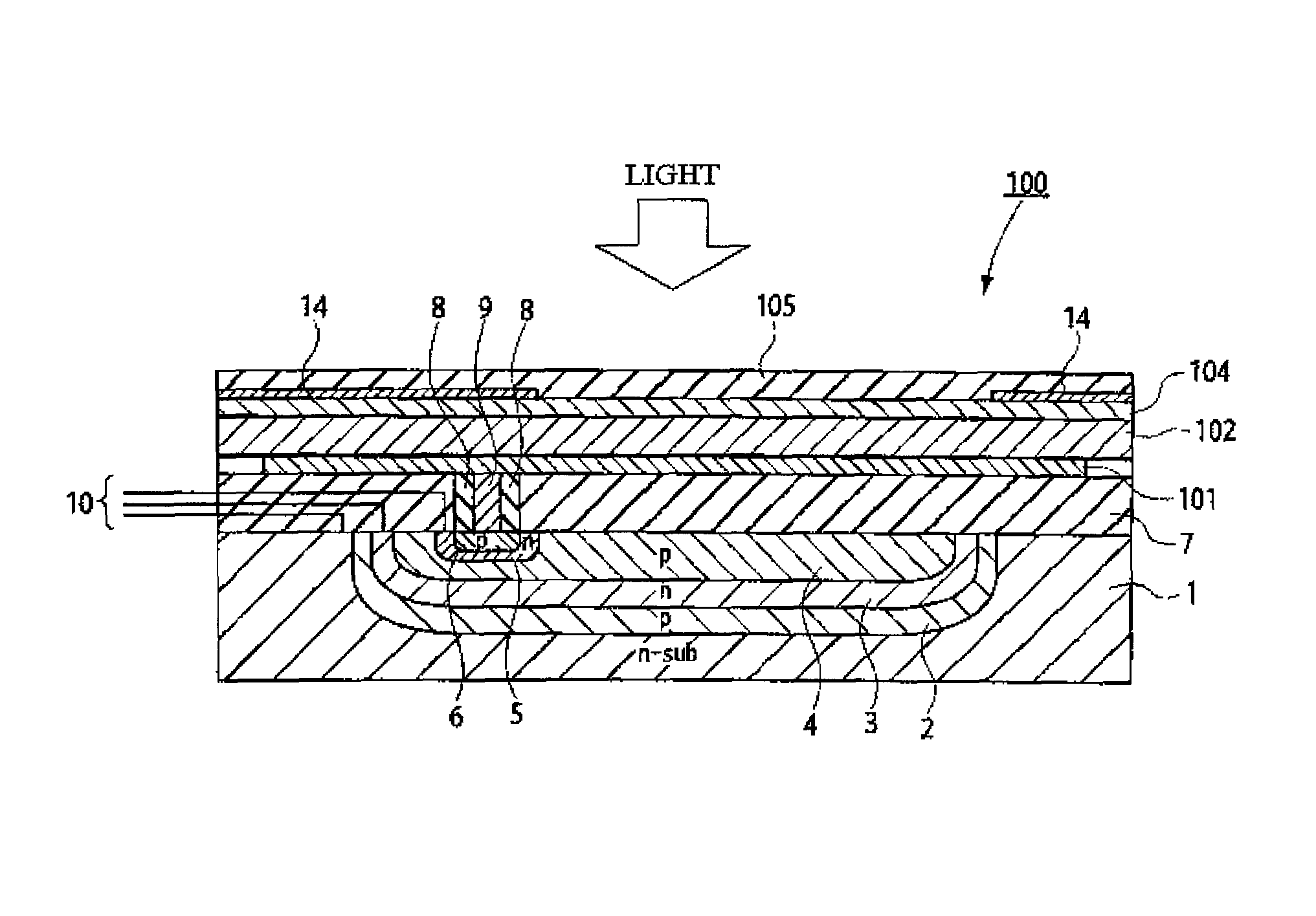
[0367]A device in the embodiment shown in FIG. 1A was fabricated. That is, amorphous ITO was deposited on a glass substrate by sputtering to a thickness of 30 nm, thereby forming a lower electrode, and Compound (A-1) was deposited thereon by vacuum heating deposition to a thickness of 100 nm to form an electron blocking layer. Thereafter, a layer formed by co-depositing Compound (1) and fullerene (C60) to a thickness of 100 nm and 300 nm, respectively, in terms of a single layer was deposited thereon by vacuum heating deposition in a state of the substrate temperature being controlled to 25° C. to form a photoelectric conversion layer. Here, the vacuum deposition of the photoelectric conversion layer was performed at a vacuum degree of 4×10⁻⁴ Pa or less.

[0368]Furthermore, amorphous ITO was deposited thereon as an upper electrode by sputtering to a thickness of 10 nm to form a transparent electrically conductive film. In this way, a solid-state imaging device having a photoelectric c...

example 2

[0371]A solid-state imaging device having a photoelectric conversion element was fabricated in the same manner as in Example 2 except that the film thickness of Compound (I) was changed to 30 nm.


PUM


Abstract

To provide a photoelectric conversion element capable of functioning as a photoelectric conversion element when a compound having a specific structure is applied to the photoelectric conversion element, causing the element to exhibit a low dark current, and reducing the range of increase in the dark current even when the element is heat-treated, and an imaging device equipped with such a photoelectric conversion element. A photoelectric conversion element having a photoelectric conversion film which is sandwiched between a transparent electrically conductive film and an electrically conductive film and contains a photoelectric conversion layer and an electron blocking layer, wherein the electron blocking layer contains a compound having, as a substituent, a substituted amino group containing three or more ring structures.

Description

TECHNICAL FIELD[0001]The present invention relates to a photoelectric conversion element, a production method thereof, a photosensor, an imaging device and their driving method. The present invention also relates to a compound useful as a material for photoelectric conversion elements.BACKGROUND ART[0002]As for the solid-state imaging device, there is widely used a flat light-receiving device where photoelectric conversion sites are two-dimensionally arrayed in a semiconductor to form pixels and a signal generated by photoelectric conversion in each pixel is charge-transferred and read out through a CCD or CMOS circuit. The conventional photoelectric conversion site generally used is a photodiode part formed using PN junction in a semiconductor such as Si.[0003]In recent years, fabrication of a multipixel device is proceeding, and the pixel size and in turn, the area of a photodiode part become small, which causes problems of reduction in the aperture ratio, reduction in the light c...

Claims


Application Information

Patent Timeline
Patent Type & Authority Patents(United States)
IPC IPC(8): H01L51/46B82Y10/00H01L27/146H01L51/00H01L51/42
CPCH01L27/14632H01L27/1462H01L51/0094B82Y10/00H01L51/0074H01L51/005H01L51/0072H01L51/0073H01L27/14647H01L51/4253H01L51/0047C07D209/86C07D219/02C07D223/22C07D265/38C07D279/26C07D279/28C07D401/14C07D405/14C07D409/14C07D413/14C07D417/14C07F7/0816Y02E10/549Y02P70/50H10K85/215H10K85/60H10K85/6576H10K85/6574H10K85/6572H10K85/40H10K30/30H10K30/00
Inventor FUKUZAKI, EIJINOMURA, KIMIATSU
Owner FUJIFILM CORP
Why Eureka
Try Eureka