Resist pattern forming method, resist pattern, crosslinkable negative resist composition, nanoimprint mold and photomask

a technology of resist pattern and crosslinkable negative resist, which is applied in the field of resist pattern forming method, crosslinkable negative resist composition, nanoimprint mold and photomask, can solve the problems of unsatisfactory resolution performance of ultrafine pattern and good nanoedge roughness at present, and achieve high resolution, high sensitivity, and high resolution.

Active Publication Date: 2015-03-03
FUJIFILM CORP
View PDF22 Cites 0 Cited by
  • Summary
  • Abstract
  • Description
  • Claims
  • Application Information

AI Technical Summary

Benefits of technology

[0012]An object of the present invention is to provide a resist pattern forming method capable of, even in the formation of an ultrafine (for example, a 1:1 line-and-space with a line width of 30 nm or less) pattern, forming a pattern satisfying high sensitivity, high resolution property (for example, high resolution and small line edge roughness (LER)) and excellent pattern profile all at the same time, a resist pattern, a crosslinkable negative resist composition, a nanoimprint mold and a photomask.
[0013]As a result of intensive studies, the present inventors have found that when a film with a specific thickness formed using a crosslinkable negative resist composition containing a polymer compound having a specific structure is patternwise exposed and then developed by using an alkali developer having a specific alkali component concentration, the above-described object can be attained.

Problems solved by technology

However, for example, the resolution performance for an ultrafine pattern and good nanoedge roughness are not satisfied at present by any of the combinations of a resist composition and the like disclosed.

Method used


Image

  • Resist pattern forming method, resist pattern, crosslinkable negative resist composition, nanoimprint mold and photomask
  • Resist pattern forming method, resist pattern, crosslinkable negative resist composition, nanoimprint mold and photomask
  • Resist pattern forming method, resist pattern, crosslinkable negative resist composition, nanoimprint mold and photomask

Examples


synthesis example 1

Synthesis of Polymer-3

[0265]In 120 mL of tetrahydrofuran (THF), 20 g of poly(p-hydroxystyrene) (VP2500) produced by Nippon Soda Co., Ltd. was dissolved, and 4.96 g of 1-adamantanecarbonyl chloride and 3.37 g of triethylamine were added thereto. The mixture was stirred at 50° C. for 4 hours, and the reaction solution was returned to room temperature. Thereafter, 100 mL of ethyl acetate and 100 mL of distilled water were added thereto and while stirring the reaction solution in ice water, an aqueous 1 N HCl solution was added little by little to the reaction solution to effect neutralization. The reaction solution was transferred to a separating funnel, and 100 mL of ethyl acetate and 100 mL of distilled water were further added. After stirring, the aqueous layer was removed, and the organic layer was washed with 200 mL of distilled water five times. The organic layer was then concentrated and added dropwise to 2 L of hexane. The powder after filtration was collected and vacuum-dried ...

examples 13 to 15

[0295]Resist patterns were formed and evaluated by the same operation as in EB Exposure Evaluation 1 except for applying the prepared negative resist solution on a Cr oxide film-deposited 6-inch wafer. The conditions for pattern formation and the evaluation results of each pattern are shown in Tables 6 and 7.

[0296]

TABLE 6DeveloperThickness ofAlkaliResistBaking ConditionsAlkaliConcentrationMode ofDevelopmentCompositionFilm CoatedAfter CoatingAfter ExposureSpecies(mass %)DevelopmentTimeExample 13Composition 130 nm150° C. × 90 sec110° C. × 90 secTMAH1.0%shower120 secExample 14Composition 230 nm150° C. × 90 sec110° C. × 90 secTMAH0.8%shower180 secExample 15Composition 130 nm150° C. × 90 sec110° C. × 90 secTMAH0.6%shower500 sec

[0297]

TABLE 7Sensitivity(μC / cm2)Resolution (nm)LER (nm)Pattern ProfileExample 13100204.5AExample 1490204.2AExample 1580204.0A

[0298]It is seen from the results in Table 7 that the resist pattern forming method according to the present invention is applicable also to...

examples 16 to 18

[0299]Exposure was performed using EUV light (wavelength: 13 nm) through a 1:1 line-and-space mask pattern with a line width of 30 nm. Coating of resist and development were performed by the same operation as in EB Exposure Evaluation 1, and the formed resist pattern was subjected to the same evaluations except for resolution. The conditions for pattern formation and the evaluation results of each pattern are shown in Tables 8 and 9.

[0300]

TABLE 8DeveloperThickness ofAlkaliResistBaking ConditionsAlkaliConcentrationMode ofDevelopmentCompositionFilm CoatedAfter CoatingAfter ExposureSpecies(mass %)DevelopmentTimeExample 16Composition 130 nm150° C. × 90 sec110° C. × 90 secTMAH1.0%shower120 secExample 17Composition 230 nm150° C. × 90 sec110° C. × 90 secTMAH0.8%shower180 secExample 18Composition 130 nm150° C. × 90 sec110° C. × 90 secTMAH0.7%shower500 sec

[0301]

TABLE 9Sensitivity (mJ / cm2)LER (nm)Pattern ProfileExample 16254.5AExample 17244.2AExample 18244.0A

[0302]It is seen from the results ...


PUM

PropertyMeasurementUnit
thicknessaaaaaaaaaa
widthaaaaaaaaaa
thicknessaaaaaaaaaa

Abstract

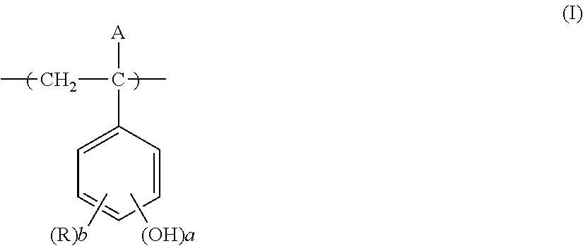
A resist pattern forming method includes: in the following order, (1) a step of forming a film on a substrate by using a negative resist composition capable of undergoing negative conversion by a crosslinking reaction; (2) a step of exposing the film; and (4) a step of performing development by using an alkali developer after the exposing, wherein the negative resist composition contains (A) a polymer compound having a repeating unit represented by the following formula (I) as defined in the specification, a thickness of the film formed in the step (1) is from 15 to 40 nm, and an alkali component concentration in the alkali developer is from 0.5 to 1.1 mass %.

Description

BACKGROUND OF THE INVENTION[0001]1. Field of the Invention[0002]The present invention relates to a resist pattern forming method suitably usable in the ultramicrolithography process such as production of VLSI or a high-capacity microchip as well as in other photofabrication processes and capable of forming a highly defined pattern by using an electron beam (EB) or an extreme-ultraviolet ray (EUV), a resist pattern, a crosslinkable negative resist composition, a nanoimprint mold and a photomask. More specifically, the present invention relates to a resist pattern forming method for use in the process where a substrate with a specific underlying film is used, a resist pattern, a crosslinkable negative resist composition, a nanoimprint mold and a photomask.[0003]The resist pattern forming method of the present invention can be also suitably used for the production method of a nanoimprint mold structure.[0004]2. Description of the Related Art[0005]In the microfabrication using a resist ...

Claims


Application Information

Patent Timeline
Patent Type & Authority Patents(United States)
IPC IPC(8): G03F7/26C08F8/14C08F12/18C08F12/24C08F12/26C08F212/14G03F1/68G03F7/00G03F7/038
CPCG03F1/68C08F12/18C08F12/24C08F12/26C08F212/14G03F7/0002C08F8/14G03F7/0382C08F212/32B82Y10/00B82Y40/00C08F212/24Y10T428/24612C08F212/22G03F1/38G03F7/039G03F7/26G03F7/30
Inventor TSUCHIHASHI, TORU
Owner FUJIFILM CORP
Why Eureka
Try Eureka