
Conjugated polymer and semiconductor devices including the same

a technology of conjugated polymers and semiconductor devices, applied in the direction of organic chemistry, sustainable manufacturing/processing, final product manufacturing, etc., can solve the problems of limited performance of some polymers in pleds, fluorescence quenching, and difficult synthesis of such materials, and achieves improved solubility in organic solvents, less cost, and convenient stacking

Inactive Publication Date: 2015-05-05
IOWA STATE UNIV RES FOUND
View PDF2 Cites 0 Cited by
  • Summary
  • Abstract
  • Description
  • Claims
  • Application Information

AI Technical Summary

Benefits of technology

This patent describes a new type of conjugated polymer that has better properties than other similar materials. It can increase the electronic affinity, electron transport, photoluminescence, oxidative stability, and thermal stability of materials that contain it. It is easier and less expensive to synthesize than other n-type semiconducting organic materials and can be functionalized to improve its solubility in organic solvents. Additionally, it has a decreased propensity for aggregation and can withstand a variety of conditions, making it more robust and easier to use in semiconductor devices. The synthetic route to generate it is simple and efficient, making it easier to scale up the procedure.

Problems solved by technology

In many instances the synthesis of such materials is difficult, preventing structural modification required for optimization of properties such as solubility, electron affinity and electron, mobility.
The performance of some polymer in PLEDs can be limited.
For example, some polymers can aggregate and cause fluorescence quenching.

Method used


Image

  • Conjugated polymer and semiconductor devices including the same
  • Conjugated polymer and semiconductor devices including the same
  • Conjugated polymer and semiconductor devices including the same

Examples


example 1.1

Synthesis and Characterization

[0163]The monomer 2,6-dihexyl-4,8-dibromobenzobisoxazole (2) was prepared by the condensation of dibromodiaminohydroquinone (1) with heptanoyl chloride in the presence of poly(trimethylsilylphosphate) (PPSE). The synthetic routes to the monomer (2) and corresponding copolymers are outlined in Scheme 1. The six new copolymers were made via Sonogashira cross-coupling of monomer (2) with the corresponding dialkynyl comonomer using palladium and copper catalysts in a mixture of diisopropylamine and toluene. These conditions yielded polymers in good yields after removal of lower molecular weight material. All of the polymers were soluble in common organic solvents such as chloroform, THF, and chlorobenzene and the 1H NMR spectra were in agreement with the proposed structures for each polymer.

[0164]

[0165]

TABLE 1Physical Properties of Benzobisoxazole Polymers.YieldMwPolymer[%]Mn [kDa]a[kDa]aPDITd [° C.]bTg [° C.]cPBOCz-O7413.023.81.8354139PBOCz-EH9547.974.91.6...

example 1.2

Optical Properties

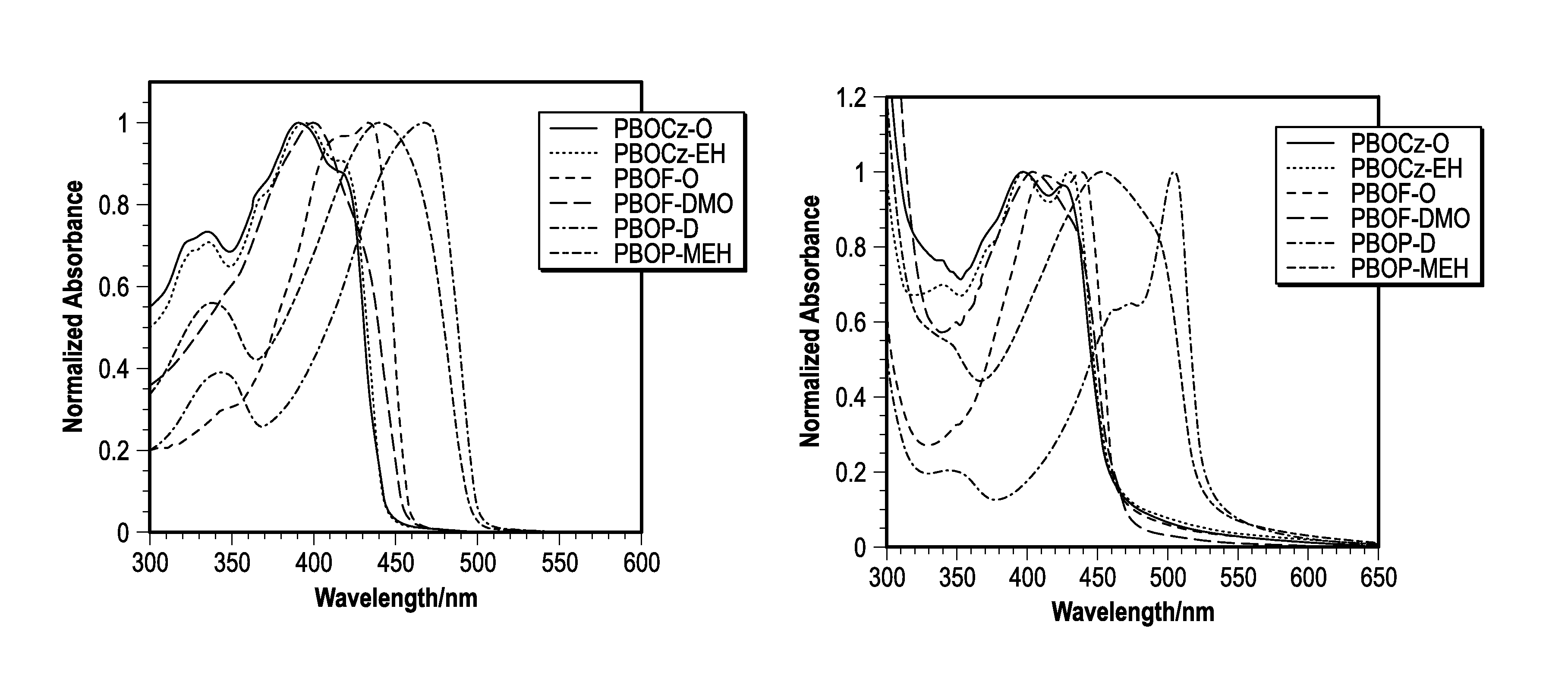
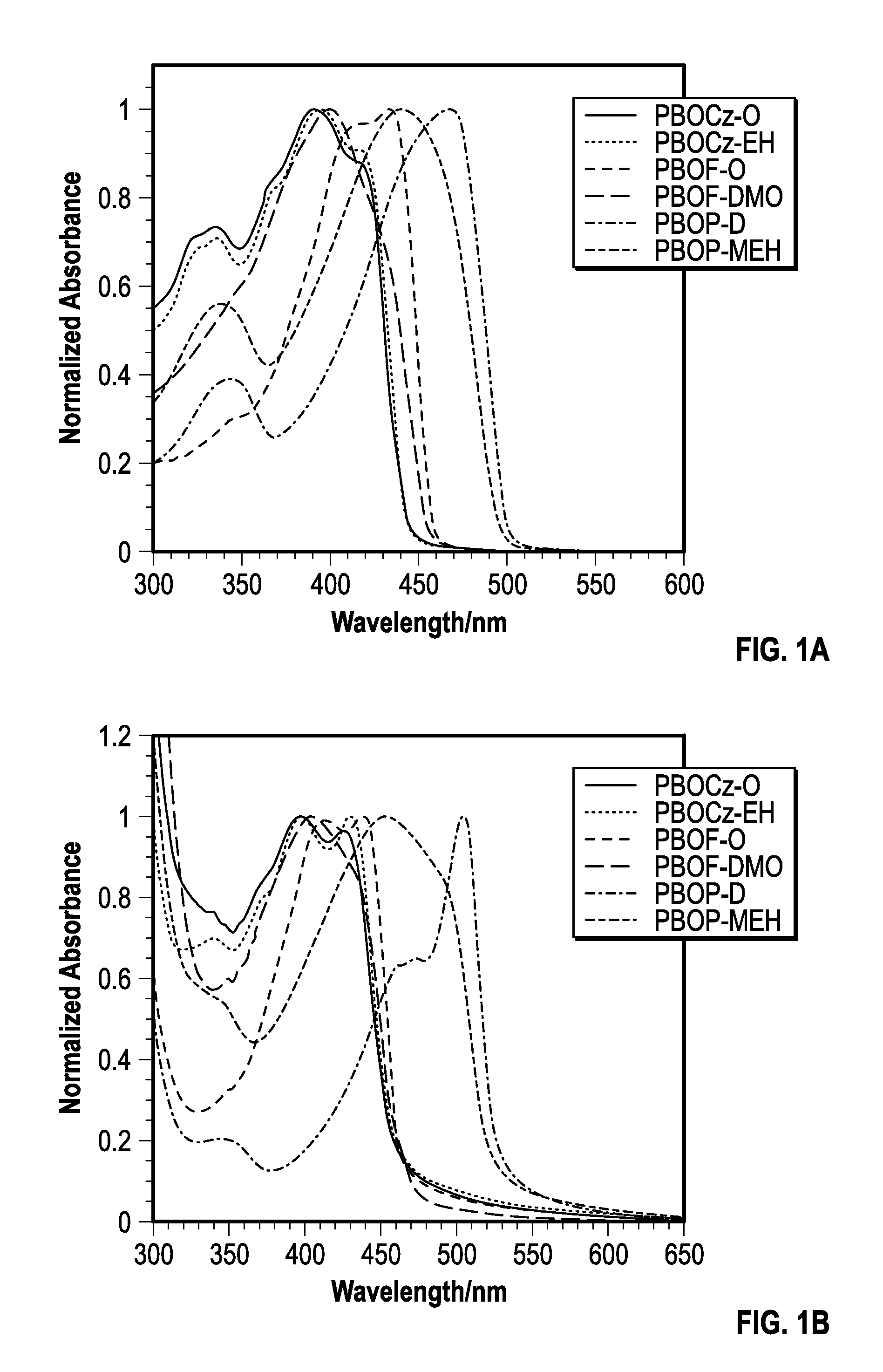
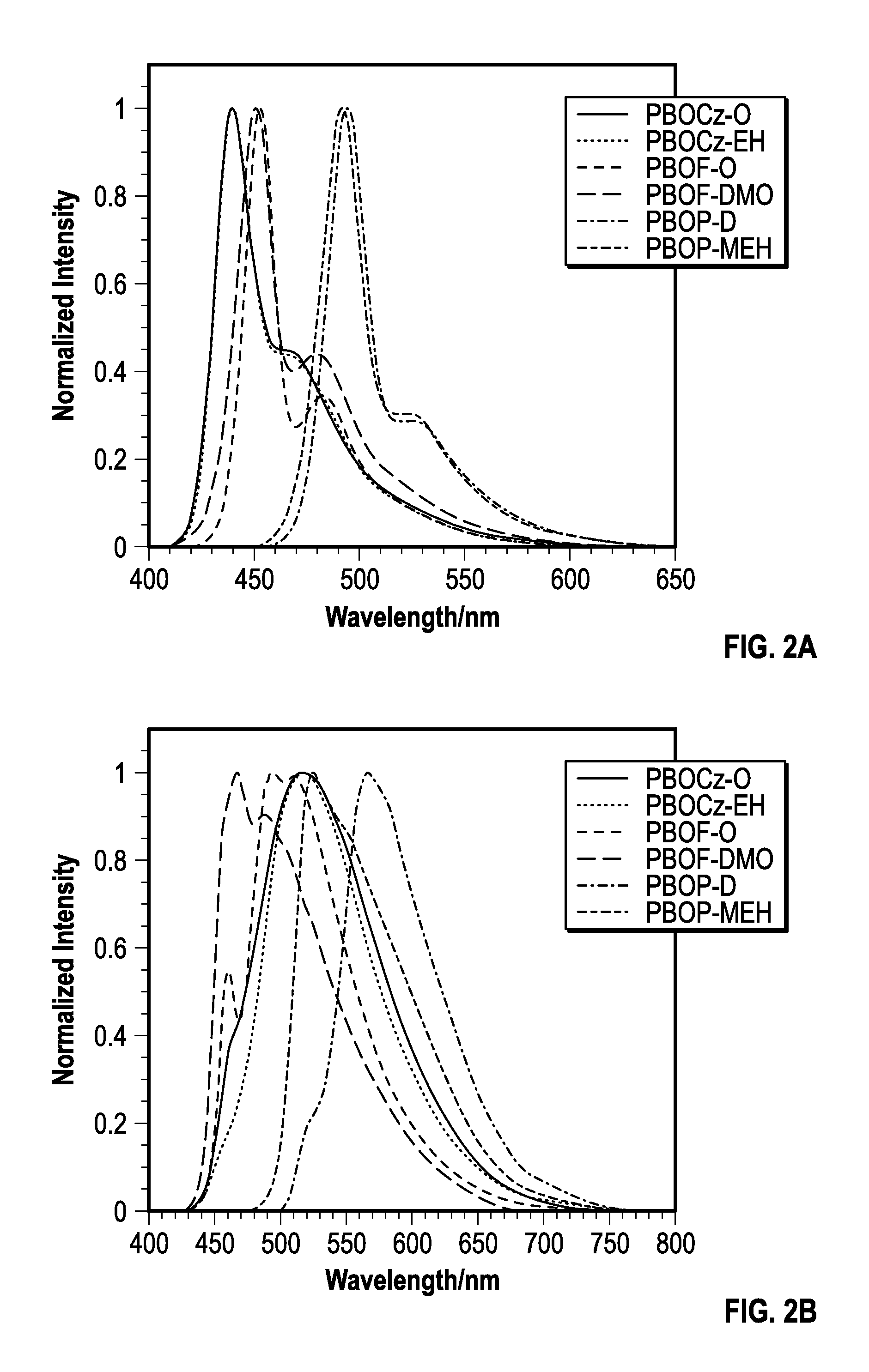
[0167]The photophysical characteristics of the polymers both in dilute solutions and thin films were examined using UV-vis absorption and fluorescence spectroscopy. The normalized absorbance spectra of the polymers in solution and films are shown in FIGS. 1a-b and the data is summarized in Table 2. The absorption profiles of PBOCz-O and PBOCz-EH were virtually identical both in solutions and films, regardless of side chain structure. In solution, these polymers had absorption maxima at 392 and 394 nm respectively, which were the shortest wavelengths of the six polymers. The absorption spectra of the carbazole polymer films showed a bathochromic shift of ˜35 nm relative to the solution spectra, which is a consequence of π-stacking between polymers in the solid state. The similarities between the PBOCz-O and PBOCz-EH spectra indicate that the branched side chain does not disrupt n-stacking any more than the linear chain. The carbazole polymers have among the largest ...

example 1.3

Ultraviolet Photoelectron Spectroscopy

[0173]The ionization potentials of the polymers were measured using ultraviolet photoelectron spectroscopy. This technique determines the HOMO energy level in organic thin films by bombarding the sample with UV photons and measuring the kinetic energies of the ejected valence electrons. Thus, the HOMO values obtained by this technique are very precise as opposed to the more commonly used technique of cyclic voltammetry, which requires the use of approximations and has a high degree of error associated with the measurements (>0.1 eV). The electron affinities (EAs) were calculated from the measured IPs using the optical band gap. These values are summarized in Table 2.

[0174]The fluorene polymers were the most electron deficient with EAs of 3.19 and 3.12 eV for PBOF-O and PBOF-DMO, respectively. The phenylene polymers were slightly more electron rich with EAs of 2.93 and 3.05 eV for PBOP-D and PBOP-MEH, respectively. The carbazoles had the lowest E...


PUM

PropertyMeasurementUnit
temperatureaaaaaaaaaa
wavelengthsaaaaaaaaaa

Abstract

The present invention relates to conjugated polymers. In various embodiments, the present invention provides a conjugated polymer including a repeating unit including a benzene ring conjugated with the polymer backbone, wherein the benzene ring is fused to two 5-membered rings, wherein each fused 5-membered ring includes N and at least one of O and S. In various embodiments, the present invention provides semiconductor devices including the polymer, and methods of making the polymer.

Description

CROSS-REFERENCE TO RELATED APPLICATION[0001]This application claims the benefit of priority to U.S. Provisional Patent Application Ser. No. 61 / 780,202, filed Mar. 13, 2013, the disclosure of which is incorporated herein in its entirety by reference.STATEMENT OF GOVERNMENT SUPPORT[0002]This invention was made with U.S. Government support under Grant No. DMR-0846607 awarded by the National Science Foundation. The U.S. Government has certain rights in this invention.BACKGROUND OF THE INVENTION[0003]Conjugated polymers (CP)s are of tremendous scientific and technological importance, due to the impact they can make in the emerging field of organic semiconductors. Due to their unique combination of semiconducting and polymer processing properties, these materials offer a potential for enormous cost savings in electronic devices. Applications include field effect transistors (FET)s, organic light emitting diodes (OLED)s and photovoltaic cells (PVC)s. The use of conjugated polymers in organ...

Claims


Application Information

Patent Timeline
Patent Type & Authority Patents(United States)
IPC IPC(8): C08F28/06H10K99/00
CPCH01L51/0036H01L51/0035H01L51/5012Y02E10/549Y02P70/50H10K85/113H10K85/111H10K50/11
Inventor JEFFRIES-EL, MALIKAINTERMANN, JEREMY J.TLACH, BRIAN C.
Owner IOWA STATE UNIV RES FOUND
Learn More