Low-dimensional material chemical vapor sensors

a technology of chemical vapor sensors and low-dimensional materials, applied in the direction of material impedance, material analysis, instruments, etc., can solve the problems of sensors incredibly fast to react to vapor analytes, little selectivity, and inability to detect analytes accurately

Inactive Publication Date: 2015-06-23
THE UNITED STATES OF AMERICA AS REPRESENTED BY THE SECRETARY OF THE NAVY
View PDF0 Cites 9 Cited by
  • Summary
  • Abstract
  • Description
  • Claims
  • Application Information

AI Technical Summary

Benefits of technology

[0015]This disclosure concerns a new class of full-spectrum chemical sensors that are able to selectively and sensitively respond to a wide variety of analytes by combining the sensing properties of each low-dimensional material in parallel. By combining the responses from each low-dimensional material, we can positively identify chemicals of interest with a never-before-seen speed and accuracy.

Problems solved by technology

The sensitivity can be enhanced by functionalizing the graphene surface, e.g. by oxidation, but these devices showed little selectivity, and functionalization introduces additional complexity to the fabrication process.
Furthermore, in the past it has been shown that 1-dimensional (1D) CNTs are quite responsive to a variety of analytes, although their response is also not selective.
Moreover, due to the atomic size and enormous surface to volume ratio of the low-dimensional films, any small adsorbate will cause an immediate electrical response, making these sensors incredibly fast to react to vapor analytes.

Method used


Image

  • Low-dimensional material chemical vapor sensors
  • Low-dimensional material chemical vapor sensors
  • Low-dimensional material chemical vapor sensors

Examples


example 1

[0025]MoS2 is mechanically exfoliated onto SiO2 / Si wafers.

[0026]Monolayer flakes are identified with a combination of optical inspection, atomic force microscopy (AFM), and Raman Spectroscopy.

[0027]Electron beam lithography with a methylmethacrylate (MMA) / polymethylmethacrylate (PMMA) layer is used to define trenches in the layer for the deposition of patterned metal contacts to the MoS2 film.

[0028]Ti / Au, Au, or Pt is deposited in the trenches by electron beam evaporation.

[0029]Similar sensor devices are made using the same methods with chemical vapor deposition (CVD) grown semiconducting single walled CNT meshes and CVD grown monolayer graphene films. The sensors are mounted into a specially built chemical sensor testing apparatus and contacts are made to the sensors using microprobe positioners.

[0030]Nitrogen gas is bubbled through a select liquid analyte and sensors are exposed to the mixture, with the concentration of analyte in the mixture controlled using a solenoid valve and ...

example 2

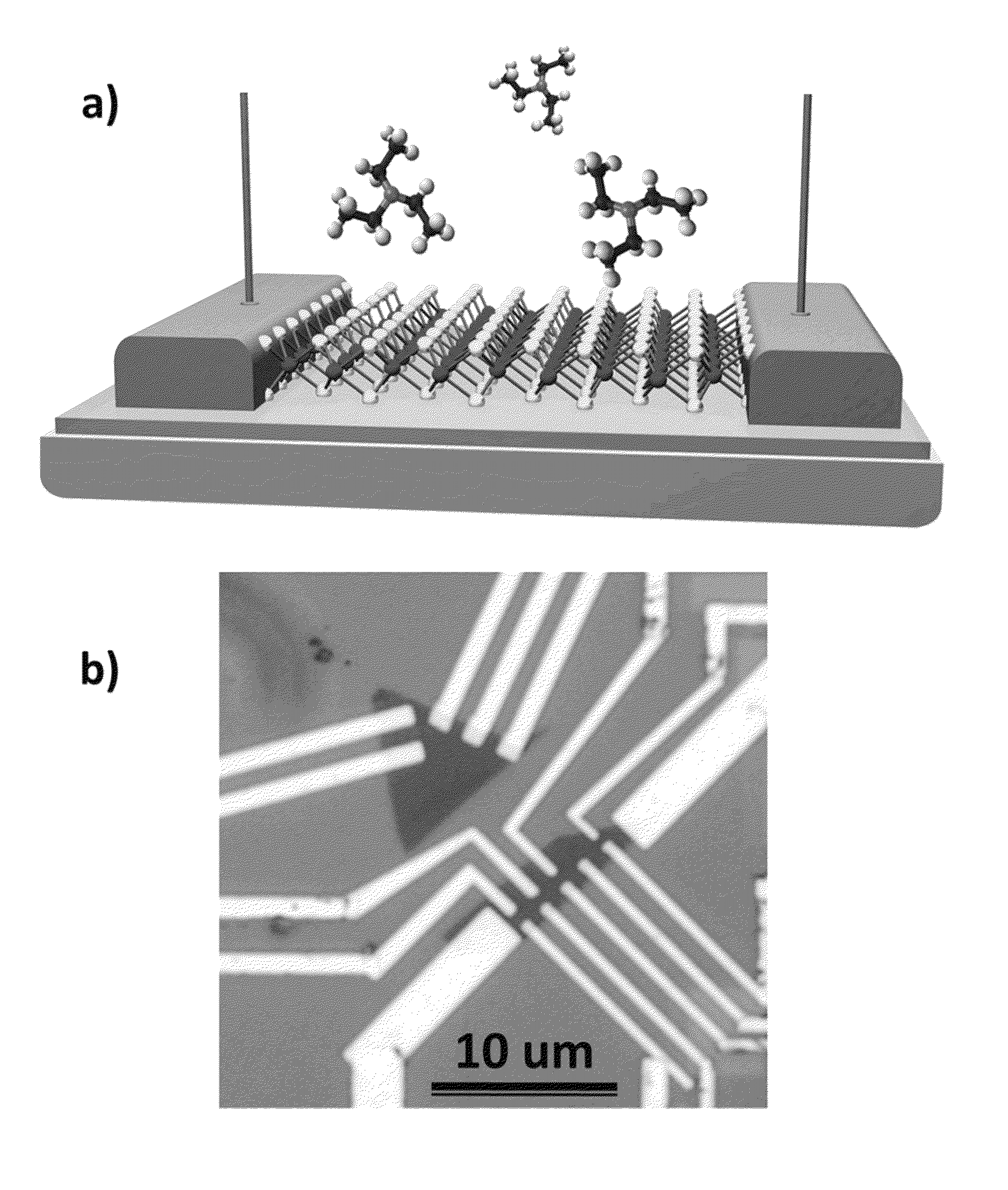
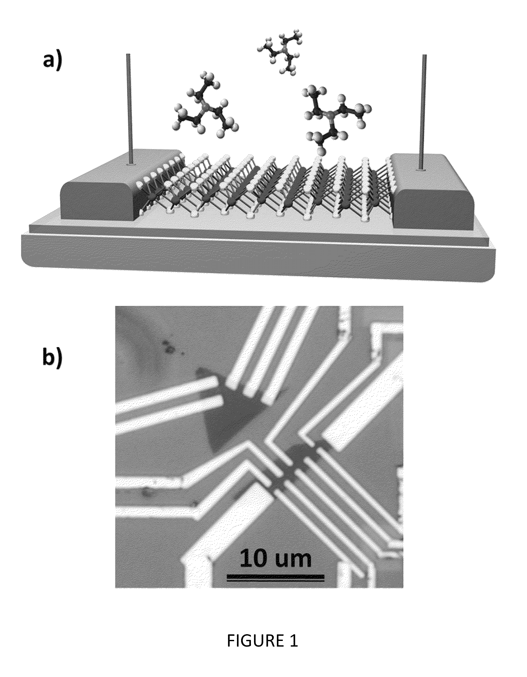
[0038]MoS2 is a layered compound with weak interaction between the layers, similar to graphite, and is widely used as a lubricant. Each layer consists of a plane of molybdenum atoms sandwiched between layers of sulfur atoms as shown in FIG. 1(a). It is relatively nonreactive at moderate temperatures (<350° C.)—it is difficult to oxidize and unaffected by dilute acids. In contrast with graphite / graphene, it is a semiconductor with an indirect bandgap (1.2 eV) and exhibits catalytic properties useful for hydrodesulfurization.

[0039]Recent work has shown that a single monolayer of MoS2 exhibits properties markedly different from the bulk: it transitions from an indirect to direct gap semiconductor (˜1.9 eV) with high luminescence efficiency and can be used as the transport channel in a field effect transistor with high on / off ratio and pronounced photoresponse.

[0040]Our sensor devices were fabricated from monolayer flakes of MoS2 that were exfoliated from bulk samples using the “Scotch ...

example 3

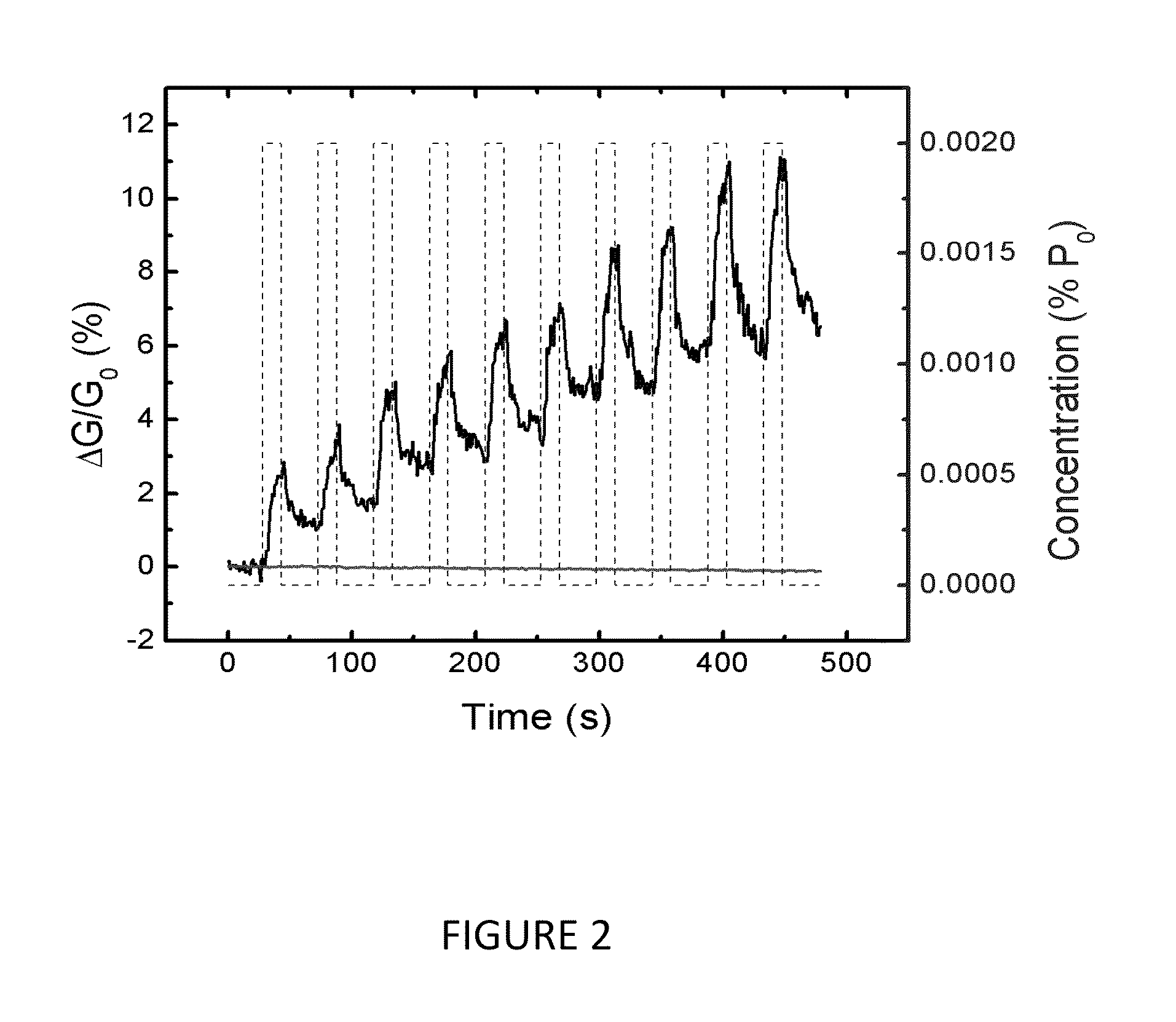
[0054]For comparison, similar data were acquired for planar sensors fabricated from (a) monolayer graphene grown by chemical vapor deposition on copper and (b) a carbon nanotube (CNT) network consisting of a dense array of CNTs forming an electrically continuous thin film, as the transport / sensor channel.

[0055]These data were recorded where AG / G0 is plotted for a sequence of TEA pulses (10 s on, 20 s off) of 0.025% P0 (12 ppm) concentration. The CNT response amplitude to a single pulse is comparable to that of the MoS2 monolayer, while that of the graphene sensor is much smaller.

[0056]However, in marked contrast with the response exhibited by the MoS2, the graphene and CNT conductivity both decrease with TEA exposure, and the data are superposed on a negatively sloped background.

[0057]The opposite response of the MoS2 and graphene / CNT sensors can be understood to first order by considering the transient charge perturbation to the sensor material upon interaction with the TEA molecul...


PUM

PropertyMeasurementUnit
thickaaaaaaaaaa
thickaaaaaaaaaa
temperaturesaaaaaaaaaa

Abstract

A method of making a low-dimensional material chemical vapor sensor comprising exfoliating MoS2, applying the monolayer flakes of MoS2 onto a SiO2 / Si wafer, applying a methylmethacrylate (MMA) / polymethylmethacrylate (PMMA) film, defining trenches for the deposition of metal contacts, and depositing one of Ti / Au, Au, and Pt in the trench and resulting in a MoS2 sensor. A low-dimensional material chemical vapor sensor comprising monolayer flakes of MoS2, trenches in the SiO2 / Si wafer, metal contacts in the trenches, and thereby resulting in a MoS2 sensor. A full spectrum sensing suite comprising similarly fabricated parallel sensors made from a variety of low-dimensional materials including graphene, carbon nanotubes, MoS2, BN, and the family of transition metal dichalcogenides. The sensing suites are small, robust, sensitive, low-power, inexpensive, and fast in their response to chemical vapor analytes.

Description

REFERENCE TO RELATED APPLICATION[0001]This application is a non-provisional of, and claims priority to and the benefits of, U.S. Provisional Patent Application No. 61 / 788,610 filed on Mar. 15, 2013, the entirety of which is herein incorporated by reference.BACKGROUND[0002]This disclosure demonstrates that single atomic layer MoS2 can be used in chemical vapor sensors and that the response is selective to analytes that are strong electron donors and some polar molecules.[0003]This disclosure demonstrates that the response of the MoS2 chemical sensors nicely complements the response to sensors fabricated from graphene and carbon nanotube (CNT) meshes. In particular, when combined, the three materials can provide a sensing suite that can correctly identify triethylamine (TEA) and acetone vapors.[0004]Furthermore, this disclosure concerns a new type of chemical sensor created from a variety of low-dimensional materials including but not limited to graphene, carbon nanotubes, and monolay...

Claims


Application Information

Patent Timeline
Patent Type & Authority Patents(United States)
IPC IPC(8): G01N27/12B82Y15/00G01N33/00G01N27/00G01N27/02
CPCG01N27/125B82Y15/00G01N33/0057Y10T29/49117Y10T436/174614G01N33/0027Y10T436/173845Y10T436/17G01N27/02G01N33/0036
Inventor FRIEDMAN, ADAM L.PERKINS, F. KEITHCOBAS, ENRIQUECAMPBELL, PAUL MJERNIGAN, GLENN G.JONKER, BEREND T
Owner THE UNITED STATES OF AMERICA AS REPRESENTED BY THE SECRETARY OF THE NAVY
Why Eureka
Try Eureka