Method for manufacturing a nanoparticle, method for manufacturing a light-emitting element having the nanoparticle, and method for manufacturing a display substrate having the nanoparticle

a technology of light-emitting elements and nanoparticles, which is applied in the field of manufacturing nanoparticles, can solve the problems of increasing the cost of manufacturing quantum dots, using expensive apparatuses, and reducing so as to reduce the cost of manufacturing nanoparticles and improve the productivity of nanoparticles. the effect of toxicity

Active Publication Date: 2015-08-18
POSTECH ACAD IND FOUND +1
View PDF16 Cites 7 Cited by
  • Summary
  • Abstract
  • Description
  • Claims
  • Application Information

AI Technical Summary

Benefits of technology

[0010]The present invention provides a method for manufacturing a nanoparticle capable of improving the productivity of the nanoparticle, a method for manufacturing a light-emitting element having the nanoparticle, and a method for manufacturing a display substrate having the nanoparticle.
[0021]According to the present invention, a nanoparticle may be formed using PEG as a solvent. PEG is cheap and less toxic, and PEG used in forming the nanoparticle may be recycled. Thus, costs for manufacturing the nanoparticle may be decreased and the productivity of the nanoparticle may be improved.
[0022]In addition, the nanoparticle formed in PEG may be used in a method for manufacturing a light-emitting element and a display substrate, and thus the productivity of the light-emitting element and the display substrate may be improved.

Problems solved by technology

The quantum dot is usually formed via a lithographic process or a gas-liquid-solid phase growth process using a catalyst, using an expensive apparatus.
However, the above-mentioned solutions are relatively expensive, increasing the cost for manufacturing the quantum dot.
In addition, octadecene and trioctylphosphine oxide are usually discarded after being used, introducing pollutants to the environment.

Method used


Image

  • Method for manufacturing a nanoparticle, method for manufacturing a light-emitting element having the nanoparticle, and method for manufacturing a display substrate having the nanoparticle
  • Method for manufacturing a nanoparticle, method for manufacturing a light-emitting element having the nanoparticle, and method for manufacturing a display substrate having the nanoparticle
  • Method for manufacturing a nanoparticle, method for manufacturing a light-emitting element having the nanoparticle, and method for manufacturing a display substrate having the nanoparticle

Examples


example 1

Manufacturing Cadmium Selenide (CdSe)

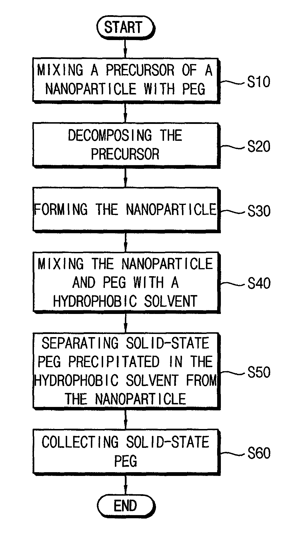
[0071]After mixing about 0.2 mmol of cadmium acetate with 1 mL of oleic acid to form a mixing solution, the mixing solution was agitated in a vacuum condition at a temperature of about 100° C., for about 1 hour. About 1 mL of trioctylphosphine (TOP) and a shot of 0.8 mmol selenium were mixed with an agitated mixing solution to form a precursor of CdSe.

[0072]Then, after heating about 4 g of PEG (the weight average molecular weight of which about 3,350) and 1 mL of oleyl amine in a nitrogen gas condition and a temperature of about 200° C. for about 1 minute to about 1 hour, the precursor of CdSe was added in the above solution including PEG and oleyl amine to manufacture CdSe having an average diameter of about 4 nm.

[0073]Obtained products were cooled at a temperature of about 60° C., and hexane was added to the obtained products to separate solid-state PEG by precipitation.

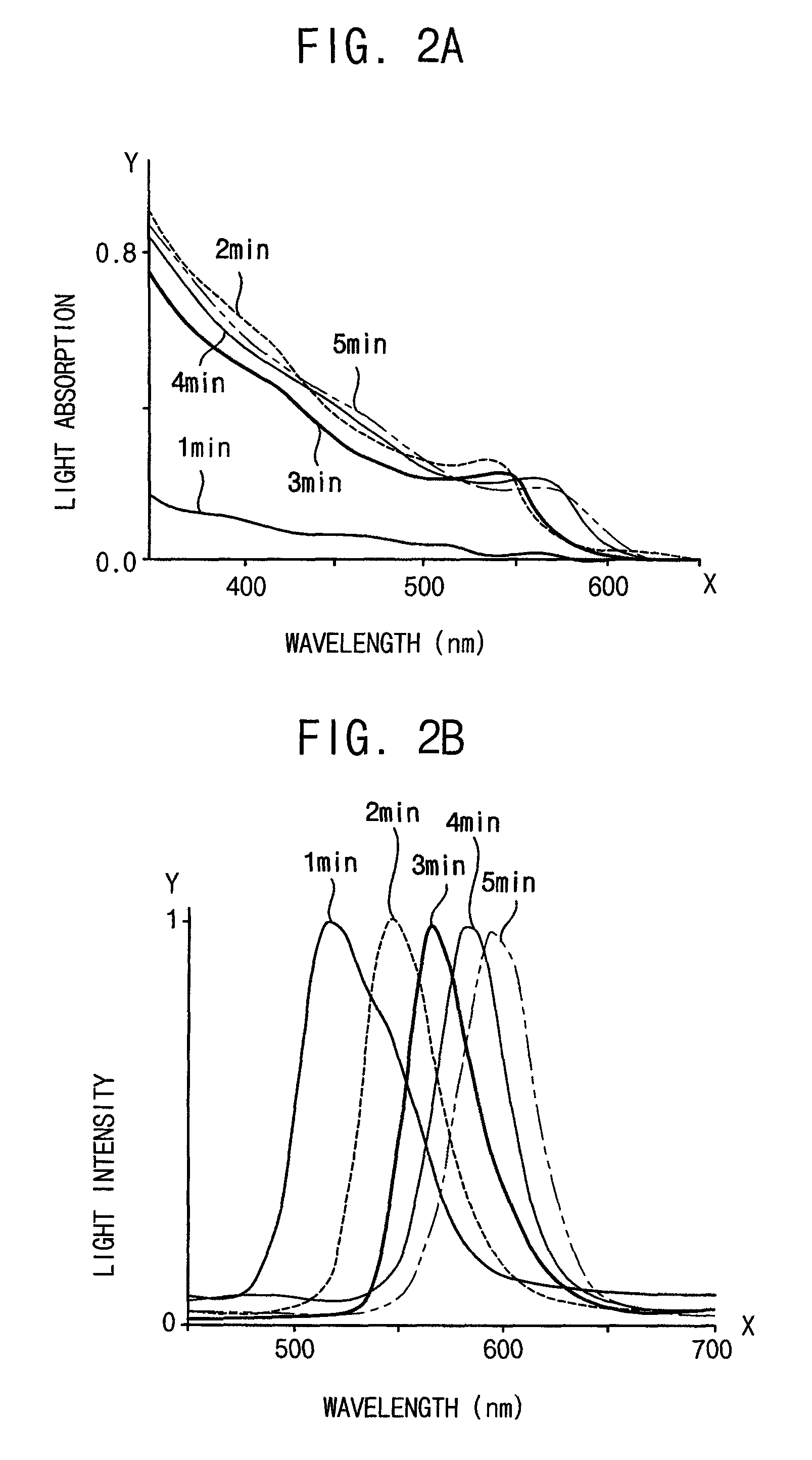
[0074]FIGS. 2A and 2B are graphs illustrating characteristics of the nanopa...

example 2

Manufacturing Indium Phosphide / Zinc Sulfide (InP / ZnS)

[0080]After preparing a mixing solution including indium acetate of about 0.4 mmol and myristic acid of about 1.7 mmol with PEG (the weight average molecular weight of about 3,350) of about 4 g, the mixing solution and PEG were agitated in a nitrogen condition which had a temperature of about 120° C., for about 1 hour. The agitated product was mixed with tris(trimethylsilyl)phosphine of about 0.2 mmol dispersed in TOP of about 0.5 ml at a temperature of about 180° C. to form a precursor of indium phosphide (InP). The precursor of InP was heated at a temperature of about 180° C. for about 3 minutes, and thus InP having the diameter of about 3.7 was formed.

[0081]Then, after a mixture including 0.3 mmol of diethyl zinc dispersed in 1 mL TOP and about 0.3 mmol bis-(trimethylsilyl)sulfide were dropped in the above products which included InP and PEG at a temperature of about 120° C., the above products including the mixture, InP and PE...


PUM

PropertyMeasurementUnit
temperatureaaaaaaaaaa

Abstract

In a method for manufacturing a nanoparticle, a precursor (e.g., transition metal complex) mixed with polyethylene glycol (PEG) is thermally decomposed. A nanoparticle is formed from the thermal decomposition. PEG is cost effective and less toxic than chemicals that are conventionally used for nanoparticle production, so that costs for manufacturing the nanoparticle may be decreased. Further, PEG may be reused to produce more nanoparticles.

Description

PRIORITY STATEMENT[0001]This application claims priority under 35 U.S.C §119 to Korean Patent Application No. 10-2008-0118717 filed on Nov. 27, 2008 in the Korean Intellectual Property Office (KIPO), the contents of which are herein incorporated by reference in their entirety.BACKGROUND OF THE INVENTION[0002]1. Field of the Invention[0003]The invention relates to a method of manufacturing a nanoparticle, a method of manufacturing a light-emitting element with the nanoparticle, and a method of manufacturing a display substrate using the nanoparticle. More particularly, the invention relates to a method of manufacturing a nanoparticle that emits light, a method for manufacturing a light-emitting element having the nanoparticle, and a method for manufacturing a display substrate having the nanoparticle.[0004]2. Description of the Related Art[0005]Generally, in the field of nanotechnology, a material or a device is made using nanosize particles (nanoparticles). “Nanoparticles,” as used ...

Claims


Application Information

Patent Timeline
Patent Type & Authority Patents(United States)
IPC IPC(8): C23C18/00C01G55/00C01G15/00C01G11/02C01G9/08C01G7/00C01G5/00C01G3/00C01B19/00C01B25/08H05B33/14C09K11/88C09K11/70C09K11/56B82Y30/00C09K11/02
CPCC09K11/02B82Y30/00C01B19/007C01B25/087C01G3/00C01G5/00C01G7/00C01G9/08C01G11/02C01G15/00C01G55/00C09K11/565C09K11/703C09K11/883H05B33/14C01P2002/84C01P2004/03C01P2004/64C01P2004/84B82B3/00H05B33/10
Inventor SHIN, JUNG-HANPARK, JAE-BYUNGPARK, HAE-ILBYUN, JIN-SEOBKIM, HYOUNG-JOOKIM, SUNG-JEEHUSSAIN, SAHIDBANG, JI-WON
Owner POSTECH ACAD IND FOUND
Why Eureka
Try Eureka