

Light emitting element and method for manufacturing same
a technology of light emitting elements and manufacturing methods, which is applied in the direction of electrical equipment, semiconductor devices, and testing/measurement of semiconductor/solid-state devices, etc., can solve the problems of small internal quantum efficiency drop, decrease in external quantum efficiency and luminance, and decrease in internal quantum efficiency. , to achieve the effect of improving the light extraction efficiency of semiconductor light emitting elements, increasing external quantum efficiency and luminance, and improving the efficiency of semiconductor light extraction
- Summary
- Abstract
- Description
- Claims
- Application Information
AI Technical Summary
Benefits of technology
Problems solved by technology
Method used
Image

Examples
example 1
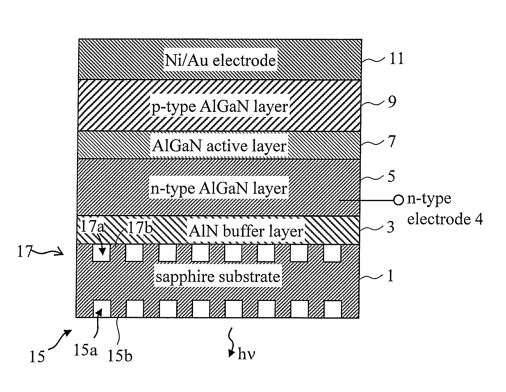
[0207]FIGS. 18 to 22 are views exemplary illustrating part of a manufacturing process for the semiconductor light emitting element (LED) shown in FIG. 1 (procedures for creating a photonic crystal structure).
[0208]First, as shown in FIG. 18, a quartz die (i.e., a master mold) 100 for creating a periodic structure is prepared. A die pattern 103 of a substrate 101 has an R / a of 0.3, a diameter of 155 nm, a period of 263 nm, and a depth of 361 nm.
[0209]The photonic crystal processing on the sapphire substrate is performed by patterning a resist through nanoimprinting, and dry-etching the sapphire through ICP etching using the resist as a mask. By the way, performing fine patterning on the order of 100 nm involves the use of a stepper such as KrF, which is problematic in that the cost will increase and failures may occur during exposure if the substrate is warped.
[0210]Meanwhile, in the nanoimprinting step, if the sapphire substrate or the nitride semiconductor layer is warped, there is...
example 2
[0221]Likewise, a quartz die 100 is prepared as shown in FIG. 18. The die pattern 103 has an R / a of 0.38, a diameter of 230 nm, a period of 299 nm, and a depth of 371 nm. As in Example 1, for the photonic crystal processing of the sapphire substrate, patterning through nanoimprinting is performed, and then, the sapphire is dry-etched through ICP dry etching using a resist as a mask. Then, as shown in FIGS. 21 and 22, it becomes possible to obtain a photonic crystal pattern with an aspect ratio of 0.5 or 0.8, as designed, that has air holes in triangular lattice arrangement on the rear surface of the sapphire substrate, and thus, a process technology was able to be established.
[0222]Next, the substrate after the dry etching is cleaned to be put into an epitaxial-growth ready state. FIG. 25 are views illustrating photographs of the shapes of the top surface and the cross section of a sapphire substrate, respectively, in the epitaxial-growth ready state. After that, crystal growth is p...
PUM
 Abstract
Description
Claims
Application Information