Printable inorganic semiconductor method

a technology of inorganic semiconductors and semiconductors, which is applied in semiconductor/solid-state device manufacturing, electric devices, solid-state devices, etc., can solve the problems of reducing the performance and acceptability reducing the performance of the resulting led, and high cost of the display. achieve the effect of high performan

Active Publication Date: 2016-06-14
X DISPLAY CO TECH LTD
View PDF67 Cites 131 Cited by
  • Summary
  • Abstract
  • Description
  • Claims
  • Application Information

AI Technical Summary

Benefits of technology

[0008]The present invention provides structures and methods that enable the construction of micro-devices formed on a sapphire substrate that can be micro-transfer printed. Such printed structures enable low-cost, high-performance arrays of electrically connected micro-devices (e.g., micro-LEDs) useful, for example, in display systems. For example, described herein are micro assembled arrays of micro devices, such as micro-LEDs, that are too small (e.g., micro LEDs with a width, length, height and / or diameter of 0.5 μm to 50 μm; e.g., a width of 1-8 μm, a length of 5-10 μm and a height of 0.5-3 μm), numerous, or fragile to be assembled by conventional means. Rather, these arrays are assembled using micro transfer printing technology. The micro-devices may be prepared on a native substrate and printed to a destination substrate (e.g., plastic, metal, glass, sapphire, transparent materials, or flexible materials), thereby obviating the manufacture of the micro-devices on the destination substrate.

Problems solved by technology

However, such displays are expensive to make, in part because of the need for small LEDs and the cost of locating small LEDs on a display substrate.
However, the lattice structure of the sapphire wafer does not match that of the GaN LED crystal and therefore the crystal structure tends to have defects, reducing the performance and acceptability of the resulting LED.
Although relatively inexpensive when compared to sapphire, silicon has an even larger lattice mismatch with the GaN crystal structures making up the LEDs than sapphire, further reducing the performance of the resulting LEDs.
However, there is no available method for undercutting a chiplet formed on a sapphire substrate to enable release of the chiplet for micro-transfer printing.

Method used


Image

  • Printable inorganic semiconductor method
  • Printable inorganic semiconductor method
  • Printable inorganic semiconductor method

Examples


Embodiment Construction

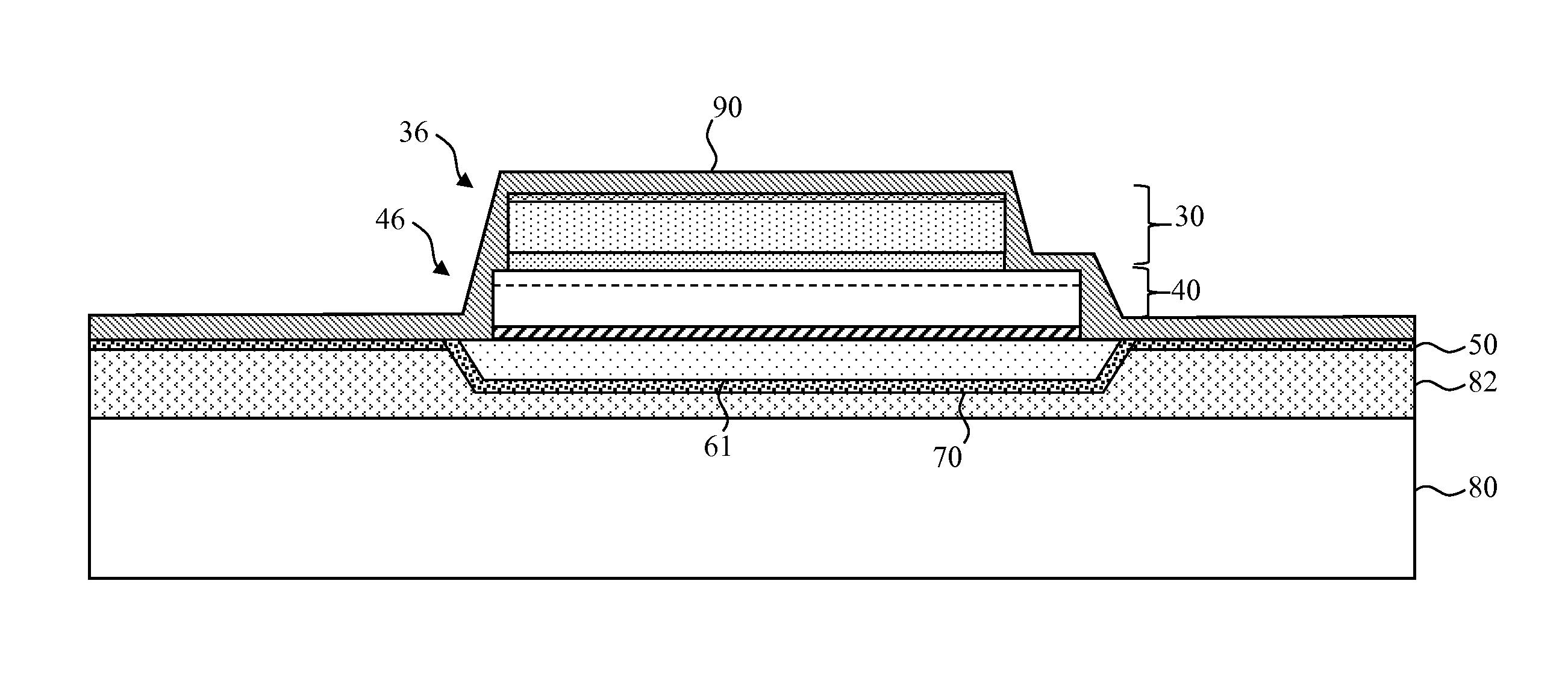
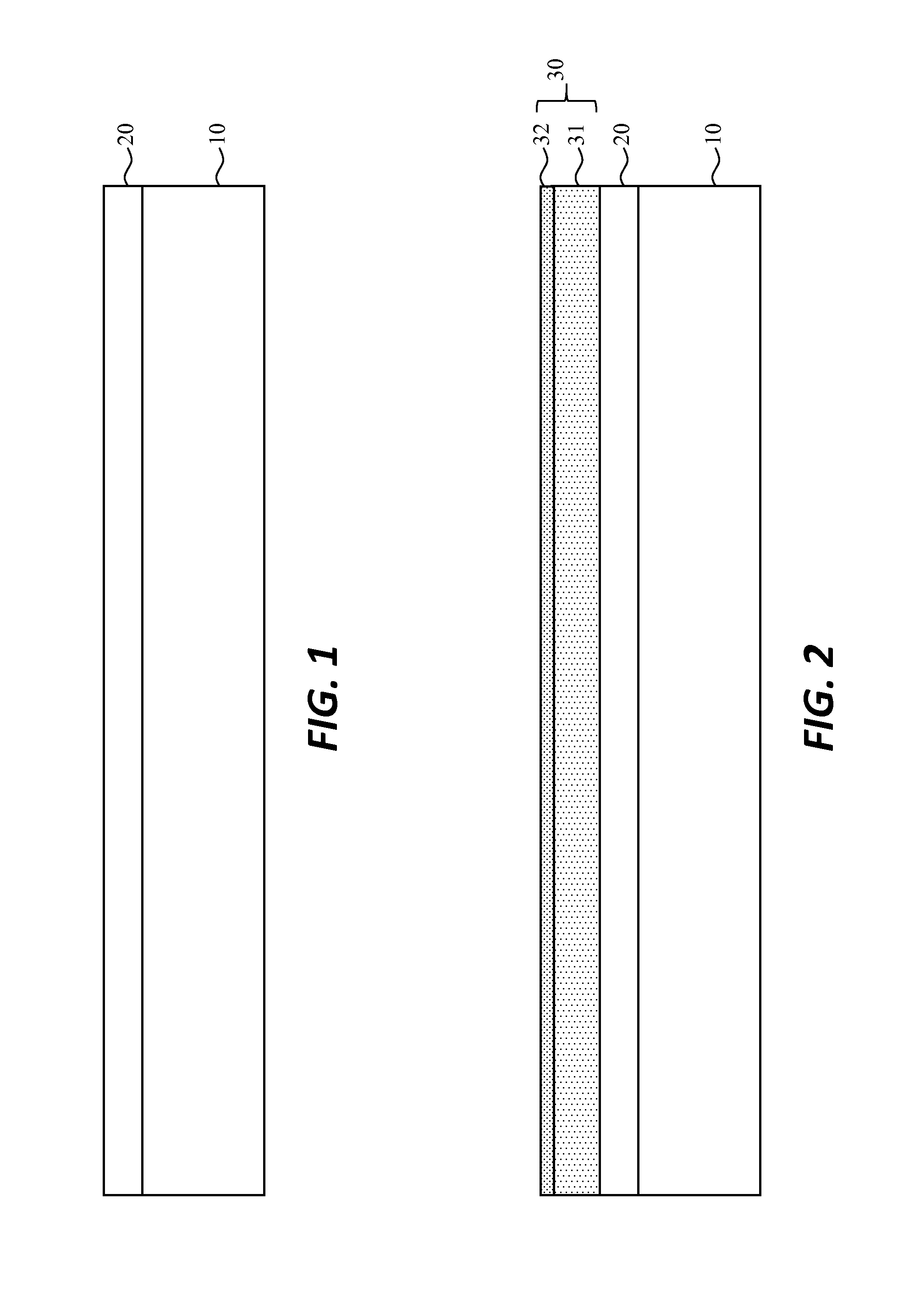
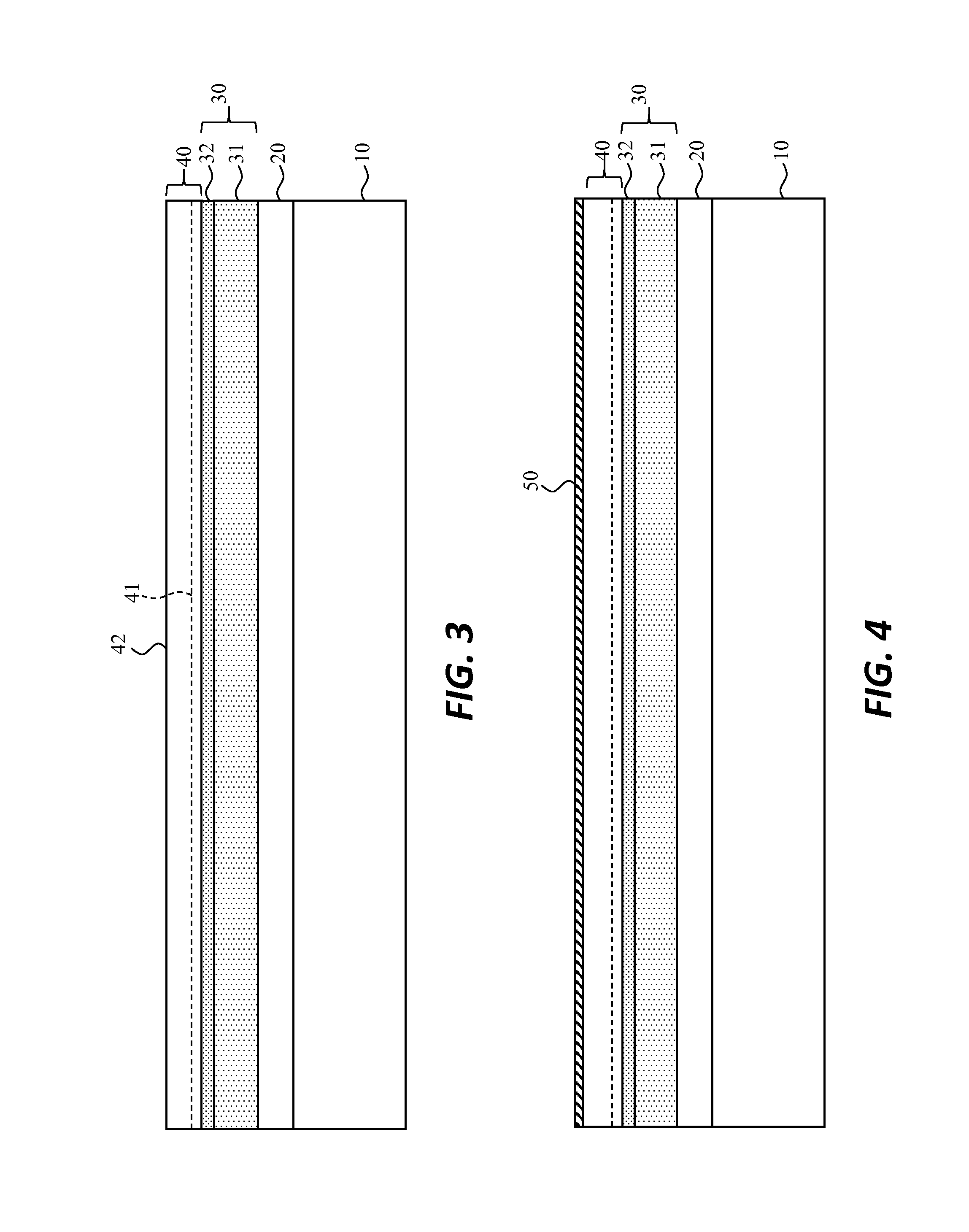
[0068]The present invention provides structures and methods that enable the construction on a substrate of micro-LED chiplets that can be micro-transfer printed. Such printed structures enable low-cost, high-performance arrays of electrically connected micro-LEDs useful, for example, in display systems. Various semiconductor elements may be formed using the methods and techniques described here, including diodes (e.g., micro-diodes), lasers (micro-lasers), and light-emitting diodes (e.g., micro-LEDs). In general, the steps of the present invention are performed using photolithographic methods known in the integrated circuit arts, for example using deposition methods including evaporation, sputtering, and coating (e.g. spin coating and curtain coating) of metals and polymers, and layer patterning methods including photoresist deposition, patterned exposure to radiation, curing, developing, etching, and stripping.

[0069]FIGS. 1-18 are diagrams illustrating the step-by-step fabrication ...


PUM

PropertyMeasurementUnit
thickaaaaaaaaaa
thickaaaaaaaaaa
thickaaaaaaaaaa

Abstract

A method of making an inorganic semiconductor structure suitable for micro-transfer printing includes providing a growth substrate and forming one or more semiconductor layers on the growth substrate. A patterned release layer is formed on the conductor layer(s) and bonded to a handle substrate. The growth substrate is removed and the semiconductor layer(s) patterned to form a semiconductor mesa. A dielectric layer is formed and then patterned to expose first and second contacts and an entry portion of the release layer. A conductor layer is formed on the dielectric layer, the first contact, and the second contact and patterned to form a first conductor in electrical contact with the first contact and a second conductor in electrical contact with the second contact but electrically separate from the first conductor. At least a portion of the release layer is removed.

Description

CROSS REFERENCE TO RELATED APPLICATIONS[0001]Reference is made to U.S. patent application Ser. No. 14 / 713,877 filed May 15, 2015, entitled Printable Inorganic Semiconductor Structure, the contents of which are incorporated by reference herein in their entirety.FIELD OF THE INVENTION[0002]The present invention relates to structures and methods for providing micro-light-emitting diodes on substrates that can be printed using massively parallel micro-transfer printing methods.BACKGROUND OF THE INVENTION[0003]Light-emitting diodes (LEDs) are widely used in the display industry as indicators and in small textual or graphic displays. More recently, LEDs are used in large, tiled outdoor displays and have been demonstrated for indoor applications. However, such displays are expensive to make, in part because of the need for small LEDs and the cost of locating small LEDs on a display substrate.[0004]LEDs are formed in a semiconductor material, often using gallium nitride (GaN). These materia...

Claims


Application Information

Patent Timeline
Patent Type & Authority Patents(United States)
IPC IPC(8): H01L21/00H01L33/40H01L33/26H01L33/20
CPCH01L33/20H01L33/40H01L33/26H01L2933/0016H01L2933/0033H01L21/6835H01L2221/68318H01L2221/68322H01L2221/6835H01L2221/68381H01L2224/24225H01L33/0093H01L29/7848H01L33/007H01L33/0095H01L33/32H01L33/36H01L33/38H01L33/44H01L33/62H01L2933/0025
Inventor MEITL, MATTHEWCOK, RONALD S.
Owner X DISPLAY CO TECH LTD
Why Eureka
Try Eureka