

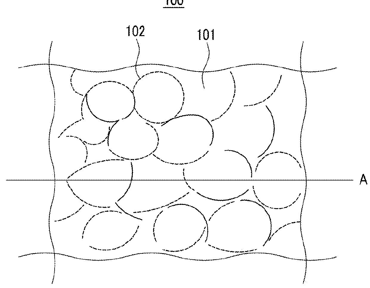
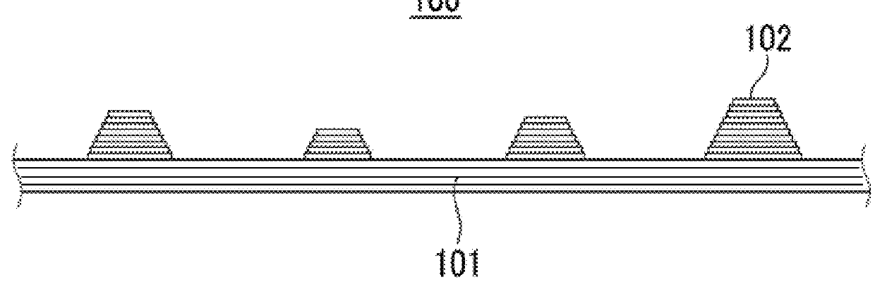
Graphene sheet, transparent electrode, active layer including the same, display, electronic device, optoelectronic device, battery, solar cell, and dye-sensitized solar cell including the electrode or active layer
a transparent electrode and active layer technology, applied in the field of graphene sheet, can solve the problems of unstable electrical characteristics of polysilicon layer, limited thin film transistors in display, and increased cost of indium tin oxide, and achieve excellent electrical and optical properties, excellent chemical excellent physical, electrical and optical properties
- Summary
- Abstract
- Description
- Claims
- Application Information
AI Technical Summary
Benefits of technology
Problems solved by technology
Method used
Image

Examples
example
Preparation of Graphene
Example 1
Formation of Graphene on SiO2 / Si Substrate
[0327]A liquid carbon source material was used to form graphene on a SiO2 / Si substrate according to the present exemplary embodiment. The SiO2 layer was 300 nm thick, and was formed by depositing SiO2 on a Si substrate.
[0328]The SiO2 / Si substrate was cleaned on the surface, and then a 100 nm-thick nickel thin film was deposited on the substrate by using an electron beam evaporator. During the deposition, the substrate was maintained at 400° C.
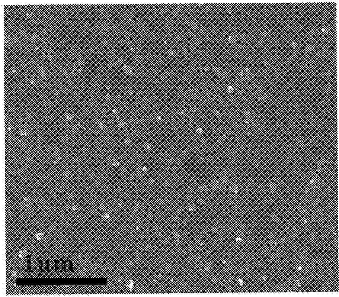
[0329]FIG. 3 shows a SEM photograph of the nickel thin film deposited in Example 1.
[0330]The SEM photograph shows that a polycrystalline nickel thin film was formed with a grain size ranging from about 50 to 150 nm (an average size of 100 nm).
[0331]The nickel thin film was heat-treated to improve the grain orientation and to increase the average grain size. The heat treatment was performed in a high-vacuum chamber, in which highly pure hydrogen was used to have a hydrogen...
example 2
[0340]A graphene sheet was formed according to the same method as Example 1 except for injecting a carbon source material into a nickel thin film at 160° C. and heat-treating the mixture.
[0341]FIG. 7 shows SEM photographs of the graphene sheet according to Example 2, and FIG. 8 shows an optical microscope photograph of the graphene sheet according to Example 2.
[0342]As shown in FIG. 7, the graphene of Example 2 had a large grain size ranging from several microns to tens of microns. The SEM photographs show a clear image luminosity contrast depending on thickness of the graphene. The lightest part is one graphene layer (C), the light part is two graphene layers (B), and the dark part is multiple graphene layers (A). The multi-graphene layers indicate ridges.
[0343]As shown in FIG. 7, the ridges have a continuous or discontinuous metal grain boundary shape. Accordingly, the ridges may have various gaps depending on the cross-sections. However, the maximum gap among the ridges is approx...
example 3
[0347]Graphene was prepared according to the same method as Example 1 except for injecting a carbon source material into a nickel thin film and heat-treating the nickel thin film at 60° C. for 10 minutes.
PUM
| Property | Measurement | Unit |
|---|---|---|
| area | aaaaa | aaaaa |
| grain size | aaaaa | aaaaa |
| grain size | aaaaa | aaaaa |
Abstract
Description
Claims
Application Information