Method for producing a resin substrate having a metal film pattern formed thereon
a metal film pattern and resin substrate technology, applied in the direction of liquid/solution decomposition chemical coatings, coatings, printing, etc., can solve the problems of low adhesive bonding strength between difficult to etch metal film patterns with high accuracy, and low heat resistance of resin film substrate and copper foil adhesive bonding. , to achieve the effect of reducing metal ion concentration, reducing metal ion drop, and excellent reliable adhesion
- Summary
- Abstract
- Description
- Claims
- Application Information
AI Technical Summary
Benefits of technology
Problems solved by technology
Method used
Image
Examples
example 1
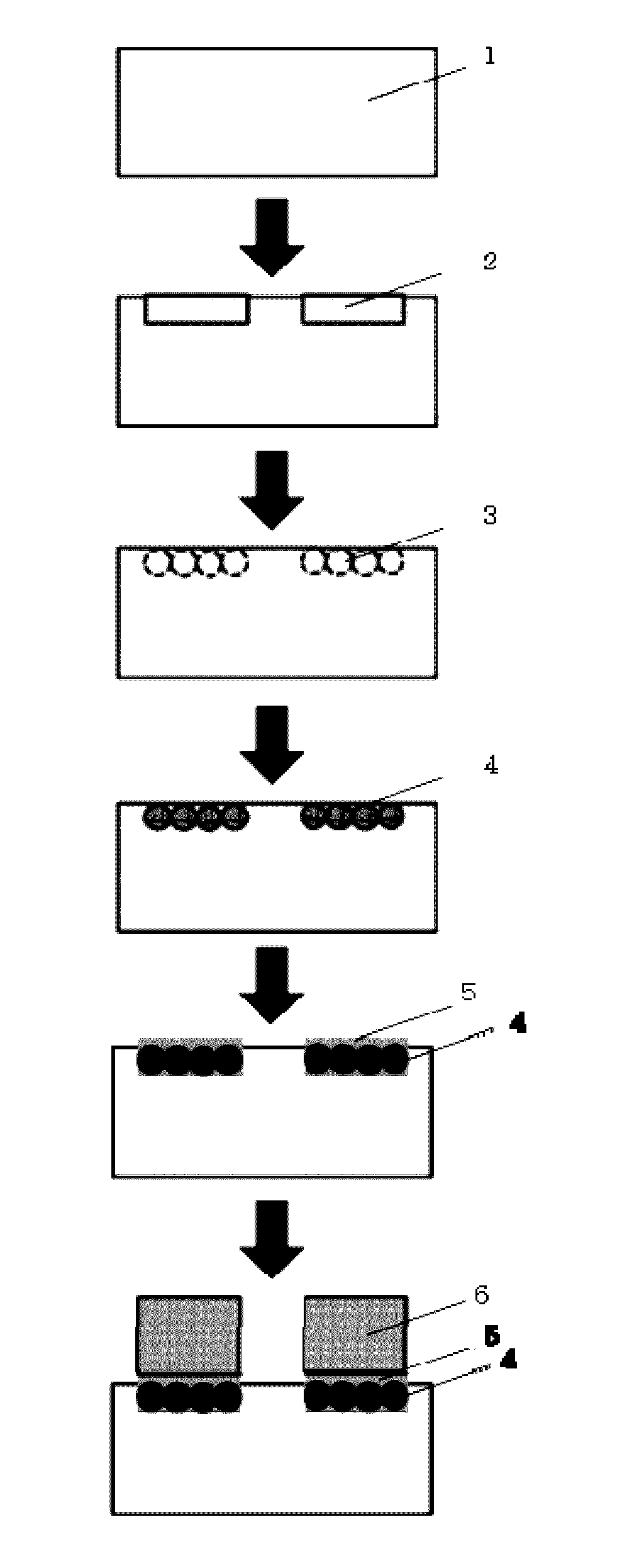
[0094]A polyimide resin substrate for printing of a latent image agent was prepared by cutting a polyimide film having a width of 30 cm and a thickness of 25 μm, brand name “Kapton H” manufactured by DU PONT-TORAY CO., LTD., to a proper size. Subsequently, pattern-printing of a latent image agent onto the surface of said polyimide resin substrate was carried out by using a gravure printer.
[0095]The latent image agent used here was prepared by adding carboxymethyl cellulose and a thixotropic agent for regulating viscosity appropriately to a solution comprising potassium hydroxide (KOH) as an alkaline compound with the alkali concentration of 3M. The viscosity of the latent image agent, measured by a cone-plate viscometer at 25° C. with a rotor rotation number of 0.5 rpm, was 370 Pa·s.
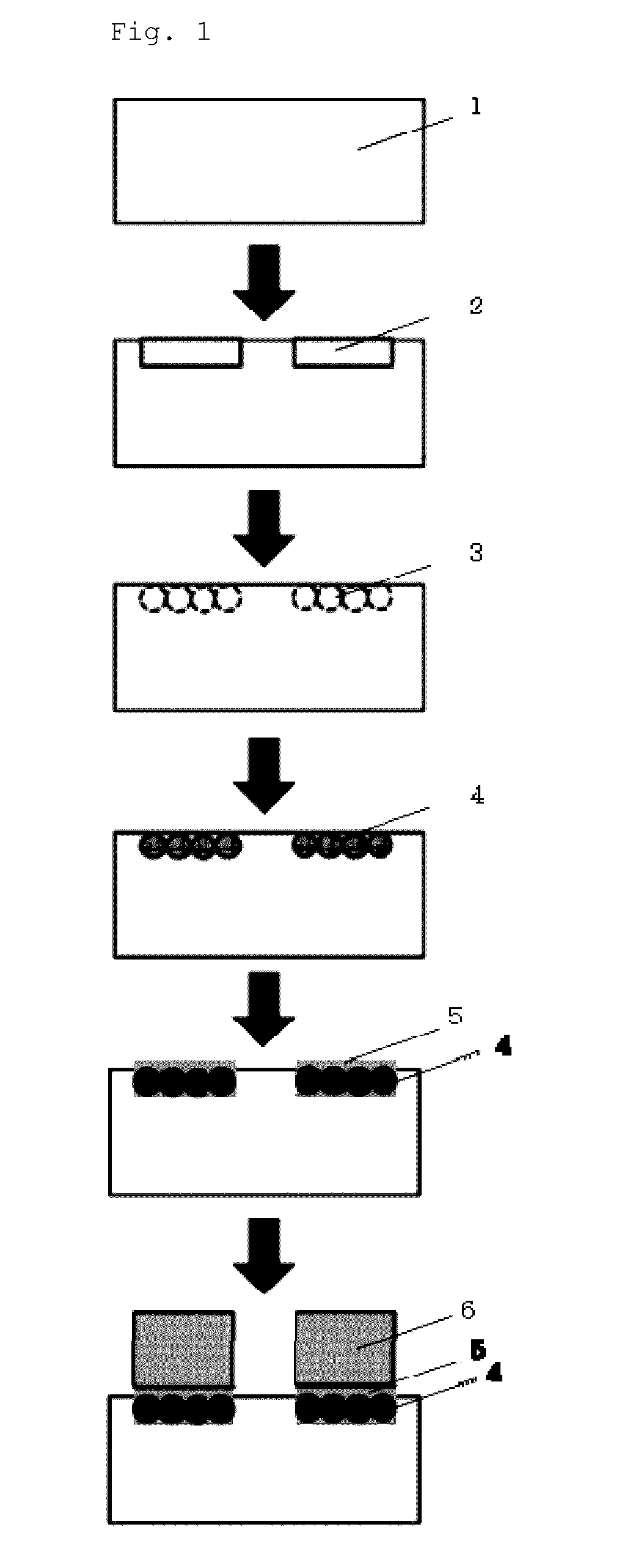
[0096]As for pattern-printing, gravure printing was carried out by using a gravure printing plate having a linear engraved groove shown in FIG. 2. The engraved groove of the gravure printing plate has a ...
example 2
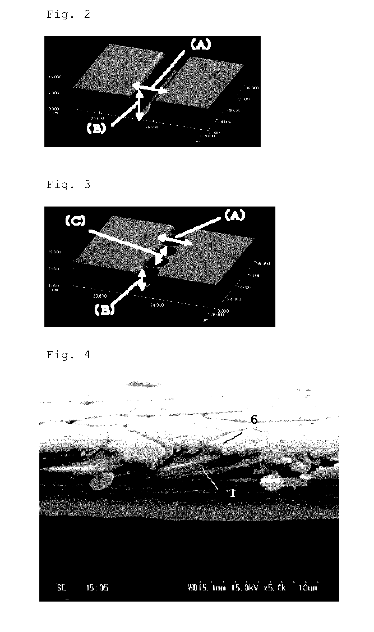
[0103]In this example, gravure printing was carried out by using a gravure printing plate having a dot-shaped engraved groove shown in FIG. 3 was used for gravure printing. The width of a side of a dot of the engraved groove of said gravure printing plate was 20 μm, the depth was 6 μm and the distance between the centers of recessed parts of the dots was 22 μm. An experiment was carried out by adjusting other conditions same as in Example 1, whereby a printed pattern having a line width of 27 μm was formed on the polyimide resin substrate.
[0104]By carrying out the same steps as in Example 1, a polyimide resin substrate on which a metal film pattern having a line width of 30 to 40 μm and a metal film thickness of 4 μm was formed was obtained.
example 3
[0105]In this example, aqueous solutions of palladium chloride having concentrations of 0.85 mM, 0.43 mM, 0.085 mM and 0.0085 mM respectively was used. Experiments were carried out by adjusting other conditions same as in Example 1 until the step of electroless nickel plating. A comparative experiment was also carried out at the same time by using an aqueous solution having a 0 mM palladium chloride concentration.
[0106]Evaluation of selective deposition of nickel plating was performed under the following standard:[0107]X; Not Deposited[0108]◯: Deposited
[0109]The result of evaluation was shown in Table 2. By the above process, selective deposition of plating was found in the modified area imprinted with a latent image agent in all the cases of using an aqueous solution of palladium chloride.
(Adhesion Test)
[0110]The samples wherein deposition of nickel plating were found in Example 3 (evaluation; ◯) were brought into an electroless copper plating process under the same conditions as i...
PUM
| Property | Measurement | Unit |
|---|---|---|
| pH | aaaaa | aaaaa |
| viscosity | aaaaa | aaaaa |
| width | aaaaa | aaaaa |
Abstract
Description
Claims
Application Information
 - R&D
- Intellectual Property
- Life Sciences
- Materials
- Tech Scout
- Unparalleled Data Quality
- Higher Quality Content
- 60% Fewer Hallucinations
Browse by: Latest US Patents, China's latest patents, Technical Efficacy Thesaurus, Application Domain, Technology Topic, Popular Technical Reports.
© 2025 PatSnap. All rights reserved.Legal|Privacy policy|Modern Slavery Act Transparency Statement|Sitemap|About US| Contact US: help@patsnap.com


