
Optical substrate, semiconductor light-emitting element and method of manufacturing semiconductor light-emitting element

a light-emitting element and semiconductor technology, applied in semiconductor devices, semiconductor/solid-state device testing/measurement, electrical devices, etc., can solve the problems of significant and disadvantageous reduction of light extraction efficiency, and achieve the enhancement improvement of internal quantum efficiency iqe, and improvement of light extraction efficiency lee

Inactive Publication Date: 2017-04-04
ASAHI KASEI KK
View PDF64 Cites 2 Cited by
  • Summary
  • Abstract
  • Description
  • Claims
  • Application Information

AI Technical Summary

Benefits of technology

The present invention provides a way to make optical substrates and semiconductor light-emitting elements that can improve both light extraction and internal quantum efficiency. This means that these elements can make more light and have more control over how the light is produced.

Problems solved by technology

As described above, in the semiconductor light-emitting element, it is impossible to extract the emitted light from the semiconductor light-emitting element, with the result that the light extraction efficiency is significantly and disadvantageously reduced.
However, since a lattice mismatch is present between a sapphire crystal and a GaN semiconductor crystal, dislocations are generated within the GaN semiconductor crystal (see, for example, non-patent document 1).

Method used


Image

  • Optical substrate, semiconductor light-emitting element and method of manufacturing semiconductor light-emitting element
  • Optical substrate, semiconductor light-emitting element and method of manufacturing semiconductor light-emitting element
  • Optical substrate, semiconductor light-emitting element and method of manufacturing semiconductor light-emitting element

Examples


example 1

[0660]On a c-plane sapphire substrate having a diameter φ2″ and a thickness of 0.33 mm, a mask material was applied by a spin coating method (2000 rpm, 20 seconds) to form a resist layer. As the mask material, an application solution was used which was diluted by propylene glycol monomethyl ether such that the solid content of a photosensitive resin composition was 5 weight %.

[0661]As the photosensitive resin composition, the followings were mixed and used: 20 weight parts of 3-ethyl-3 {[3-ethyloxetan-3-yl) methoxy] methyl} oxetane (OXT-221, made by Toagosei Co., Ltd.); 80 weight parts of 3′,4′-epoxy cyclohexane carboxylic acid-3,4-epoxy cyclohexyl methyl (Wako Pure Chemical Industries, Ltd.); 50 weight parts of phenoxy diethylene glycol acrylate (Aronix (registered trademark) M-101A, made by Toagosei Co., Ltd.); 50 weight parts of ethylene oxide-modified bisphenol A diacrylate (Aronix (registered trademark) M-211B, made by Toagosei Co., Ltd.); 8 weight parts of DTS-102 (made by Mid...

example 2

[0672]In the production of the optical substrates (A) to (C) according to example 1, the same operation was performed to produce the sapphire substrates except that the inverted resin molds (1) to (3) were changed to the resin molds (1) to (3). The surface and the cross section of the obtained sapphire substrates were observed with a scanning electron microscope.

[0673]The sapphire substrate (D) produced by using the resin mold (1) had an average concave portion depth Dave of 105 nm and an average interval Pave of 200 nm. The minimum value of the concave portion depth dn was 0 nm because it is estimated that it was the part to which no pulse was applied. For the minimal concave portion corresponding to dn=0 nm, the bottom portion of the minimal concave portion was observed. Since roughness was observed in the bottom portion, the outline of the minimal concave portion was able to be observed to be substantially circular. That is, dn=0 nm does not mean that there is nothing in the part...

example 3

Production of a Semiconductor Light-Emitting Element

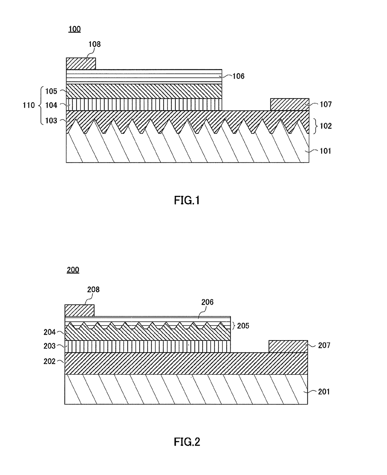
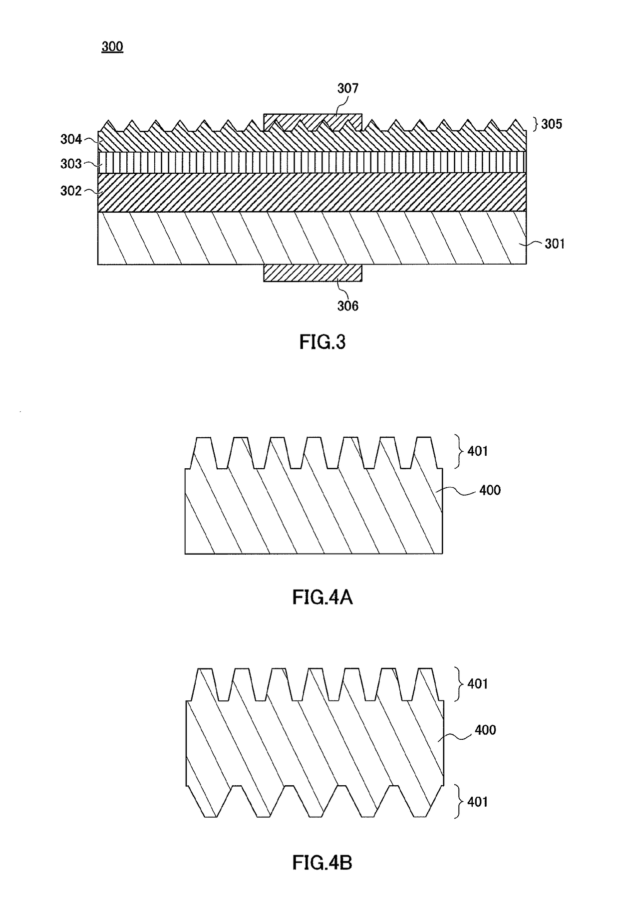
[0687]On the sapphire substrates (the optical substrates (A) to (F)) obtained in examples 1 and 2, the followings were continuously deposited by a metal organic chemical vapor deposition method (MOCVD): (1) AlGaN low-temperature buffer layer, (2) n-type GaN layer, (3) n-type AlGaN clad layer, (4) InGaN light-emitting layer (MQW), (5) p-type AlGaN clad layer, (6) p-type GaN layer and (7) ITO layer, and the semiconductor light-emitting element (A) was produced. The concave and convex portions on the sapphire substrate were embedded and flattened under conditions of film formation when the (2) n-type GaN layer was deposited. Then, the semiconductor light-emitting element (A) was etched, and an electrode pad was attached. In this state, a prober was used to pass a current of 20 mA between a p-electrode pad and an n-electrode pad, and the light emission output of the semiconductor light-emitting element (A) was measured. The light emiss...


PUM


Abstract

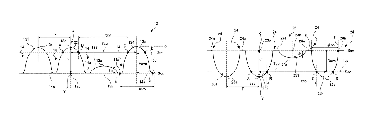
In an optical substrate (1), a concave-convex structure (12) including a plurality of independent convex portions (131 to 134) and concave portions (14) provided between the convex portions (131 to 134) is provided in a surface. The average interval Pave between the adjacent convex portions (131 to 134) in the concave-convex structure (12) satisfies 50 nm≦Pave≦1500 nm, and the convex portion (133) having a convex portion height hn satisfying 0.6 h≧hn≧0 h for the average convex portion height Have is present with a probability Z satisfying 1 / 10000≦Z≦1 / 5. When the optical substrate (1) is used in a semiconductor light-emitting element, dislocations in a semiconductor layer are dispersed to reduce the dislocation density, and thus internal quantum efficiency IQE is improved, and a waveguide mode is removed by light scattering and thus the light the extraction efficiency LEE is increased, with the result that the efficiency of light emission of the semiconductor light-emitting element is enhanced.

Description

TECHNICAL FIELD[0001]The present invention relates to an optical substrate, a semiconductor light-emitting element and a method of manufacturing a semiconductor light-emitting element. More particularly, the present invention relates to an optical substrate in which a concave-convex structure is formed in its surface, a semiconductor light-emitting element using it, a method of manufacturing it and a method of preferably managing them.BACKGROUND ART[0002]In recent years, in order to enhance efficiency in semiconductor light-emitting elements such as an OLED, a fluorescent member and an LED, the improvement of the efficiency of extracting light from the semiconductor light-emitting element has been examined. The semiconductor light-emitting element described above has a structure in which a high refractive index region including a light-emitting portion therewithin is sandwiched between low refractive index regions. Hence, light emitted by the light-emitting portion of the semiconduc...

Claims


Application Information

Patent Timeline
Patent Type & Authority Patents(United States)
IPC IPC(8): H01L33/58H01L21/66H01L33/22H01L33/32H01L21/02H01L33/00H01L33/20
CPCH01L33/58H01L22/12H01L33/22H01L21/0243H01L21/0254H01L21/02658H01L33/007H01L33/20H01L33/32
Inventor KOIKE, JUNMITAMURA, YOSHIMICHIYAMAGUCHI, FUJITO
Owner ASAHI KASEI KK
Learn More