Method of manufacturing the thin film

a manufacturing method and thin film technology, applied in the direction of basic electric elements, electrical equipment, semiconductor devices, etc., can solve the problems of difficult control of two, low resistivity of the surface of the formed substrate, and worse performance than the first, so as to reduce the change of capacity, and reduce the effect of defect density

Active Publication Date: 2017-11-21
SHENYANG SILICON TECH
View PDF3 Cites 10 Cited by
  • Summary
  • Abstract
  • Description
  • Claims
  • Application Information

AI Technical Summary

Benefits of technology

[0025]3. The advantage of the amorphous silicon technology of present invention is high defect density, and the application of the amorphous silicon layer of high thermal stability is compatible with the bonding process. Block the potential under the oxide layer, limit the changes of capacity and reduce the generated harmonic power.
[0026]4. Amorphous layer high-resistivity SOI substrate reduces RF substrate loss, amorphous layer+high-resistivity silicon increase the linearity of the substrate, amorphous layer high-resistivity SOI substrate reduces the DC voltage bias, and is compatible with CMOS, reduces RF loss.
[0027]5. The present invention can manufacture high-quality components with low manufacturing cost.

Problems solved by technology

1. SOQ (silicon on quartz), SOS (silicon on sapphire): SOQ is as same as traditional SOI (silicon-on-insulator), which generate a lower leakage current, since its lower parasitic capacitance, the circuit performance under high frequency is enhanced. The advantage of SOS is its extremely good electrical insulation, which can effectively prevent radiation caused by stray currents from spreading to nearby elements. The substrates like SOQ and SOS can get excellent RF performance, but this kind of structure is very rare, so they are very expensive.
2. High-resistivity silicon substrates: the resistivity of it is more than 500 ohm·cm, this kind of substrate is worse than the first, this kind of substrate is not benefiting from the structure advantages of SOI type, but they cost less.
3. High-resistivity SOI substrate: this kind of substrate has structural advantages, but the performance is worse than the first.
However, the diffusion of oxygen atoms and the process of heat treatment lead to the low resistivity of the surface of the formed substrate.
It is difficult to control the two reasons now.
4. Based on the 3, the high-resistivity SOI substrate is improved by adding defect layer: to achieve the purpose, lots of techniques are tried, but there are some disadvantages: sensitive to SOI manufacturing and generating heat in the subsequent process of IC components fabrication, not easy to make materials with good thermal stability.

Method used


Image

  • Method of manufacturing the thin film
  • Method of manufacturing the thin film

Examples


embodiment 1

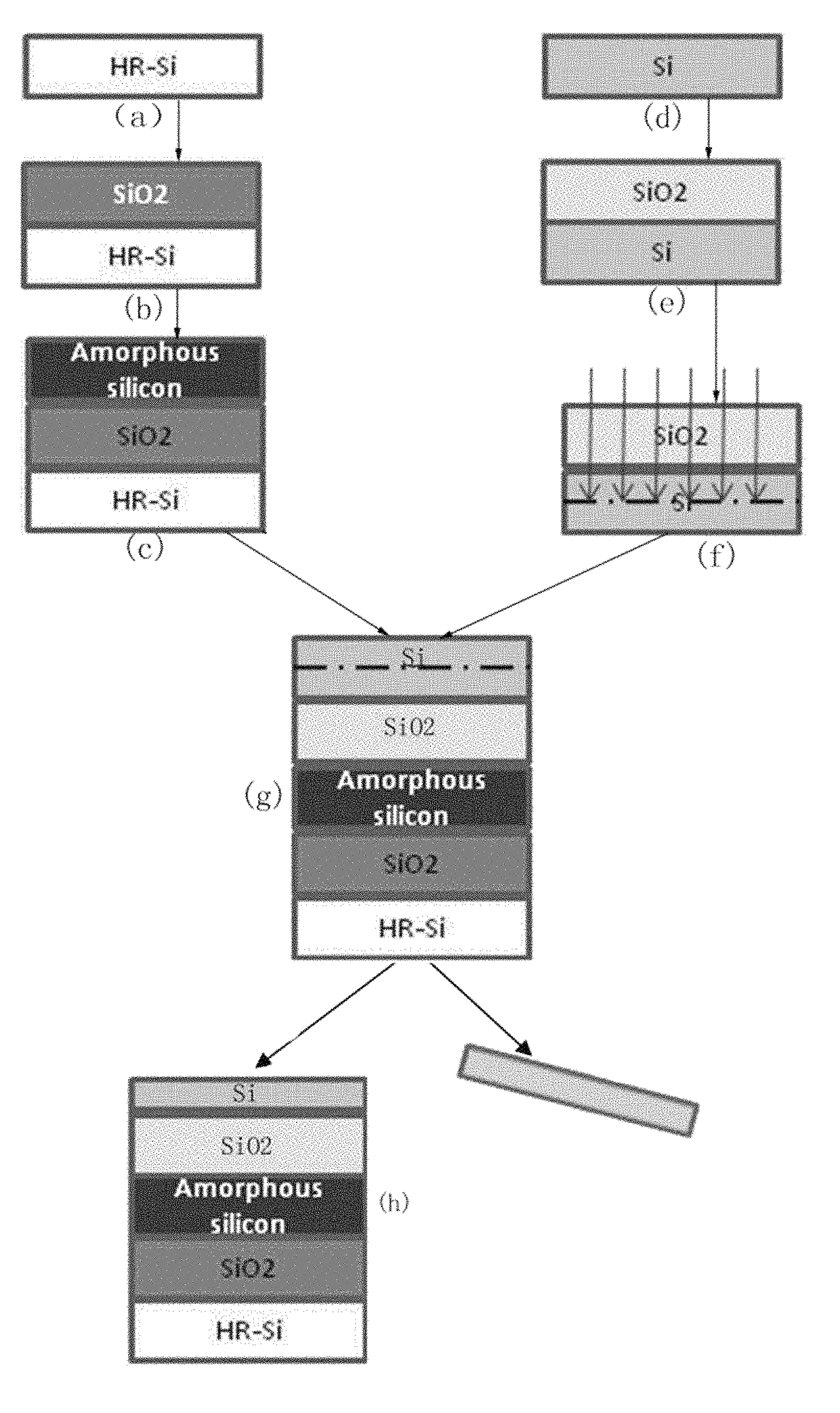
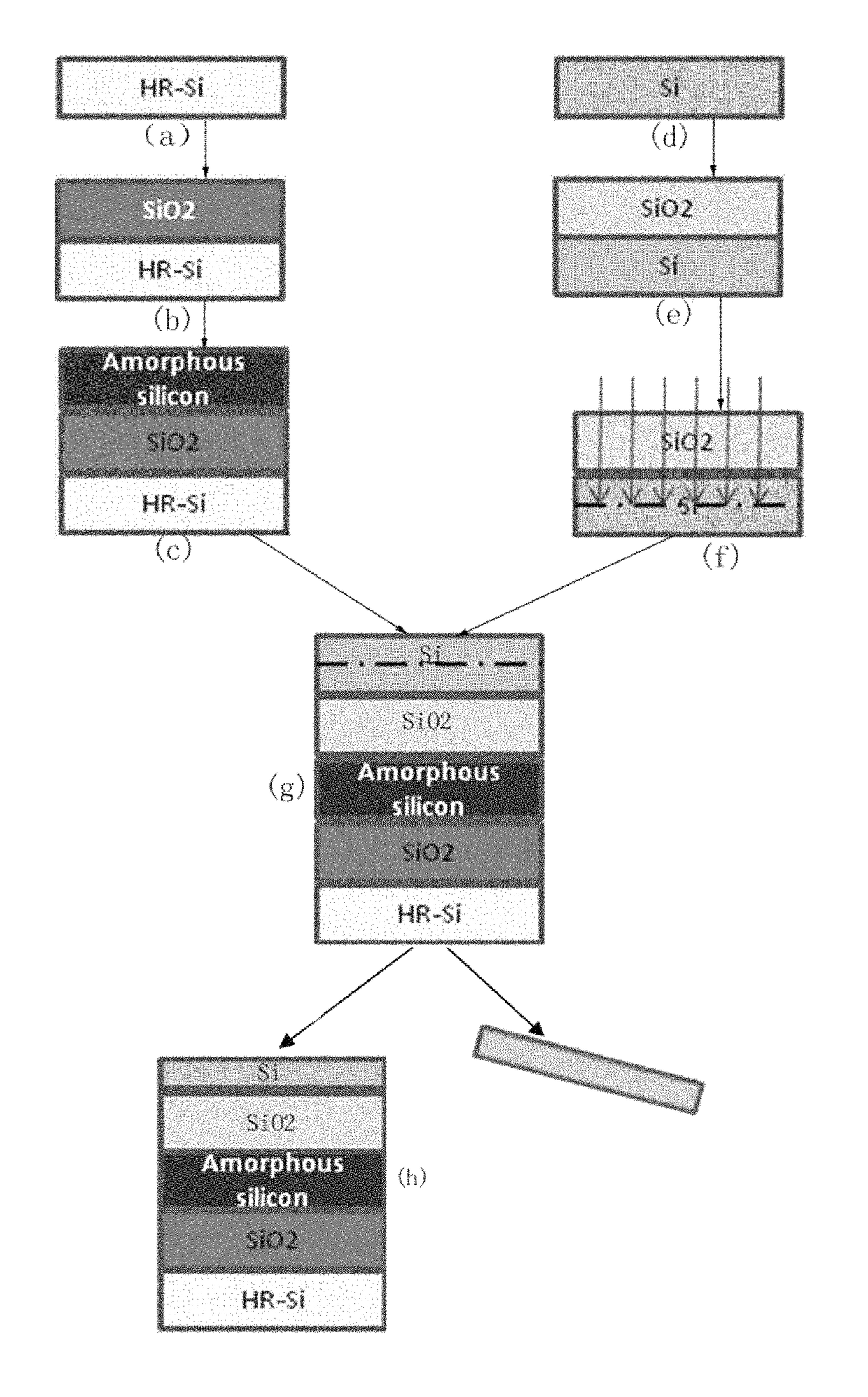
[0030]The present embodiment provides a method of manufacturing thin film, wherein the thin film is a SOI wafer with amorphous silicon layer, and the manufacture includes the steps below:

[0031]1. Provide a high-resistivity silicon wafer, of which the resistivity is greater than 1000 ohm·cm, and clean its surface by using DHF, SC1 and SC2 in order, to remove the natural oxidation layer and the pollutant on the surface of the silicon wafer; using the test apparatus to test the condition of particles on the surface of silicon wafer, the silicon wafers which meet the requirement will come into the next step (FIG. 1(a)).

[0032]2. Refer to FIG. 1(b), manufacture silicon oxide layer on the surface of high-resistivity silicon wafer, the thickness of the grown oxide layer is about 200 angstroms; the process for manufacturing is that: put the high-resistivity silicon wafer in the oxidation oven, the oxidation temperature is about 1100° C., then clean by using SC1 and SC2 in order, to remove th...


PUM

PropertyMeasurementUnit
thicknessaaaaaaaaaa
thicknessaaaaaaaaaa
thicknessaaaaaaaaaa

Abstract

The invention disclosed a method of manufacturing the thin film, which belongs to the technological field of SOI wafer manufacture. By growing a layer of dielectric material (silicon oxide) on the provided high-resistivity silicon wafer, then to grow a layer of amorphous silicon on the dielectric material, to transfer a layer of silicon oxide to the amorphous silicon, to make the mono crystalline silicon exist on the oxidation layer, so that a SOI wafer with a layer of amorphous silicon is manufactured. The process above is completed in specific process conditions. The manufactured thin film, e.g. SOI wafer with amorphous silicon layer, is used main for RF apparatus.

Description

TECHNICAL FIELD[0001]The present invention relates to the field of the manufacture technology of SOI wafer, more particularly relates to a method of manufacturing the thin film, the manufactured film is used main for RF apparatus.BACKGROUND TECHNOLOGY[0002]Materials currently used in RF front end modules are as follows:[0003]1. SOQ (silicon on quartz), SOS (silicon on sapphire): SOQ is as same as traditional SOI (silicon-on-insulator), which generate a lower leakage current, since its lower parasitic capacitance, the circuit performance under high frequency is enhanced. The advantage of SOS is its extremely good electrical insulation, which can effectively prevent radiation caused by stray currents from spreading to nearby elements. The substrates like SOQ and SOS can get excellent RF performance, but this kind of structure is very rare, so they are very expensive.[0004]2. High-resistivity silicon substrates: the resistivity of it is more than 500 ohm·cm, this kind of substrate is w...

Claims


Application Information

Patent Timeline
Patent Type & Authority Patents(United States)
IPC IPC(8): H01L21/00H01L21/306H01L21/30H01L21/265H01L21/324H01L21/02
CPCH01L21/0262H01L21/02065H01L21/02592H01L21/02532H01L21/324H01L21/26513H01L21/3003H01L21/30625H01L21/02H01L21/02041H01L21/02107H01L27/1203H01L21/76254H01L21/7624
Inventor SUN, WEI
Owner SHENYANG SILICON TECH
Why Eureka
Try Eureka