
Scan control for scanning probe microscopes

a scanning probe and microscope technology, applied in the direction of material analysis using wave/particle radiation, generators/motors, instruments, etc., can solve the problems of asymmetric scan pattern, linear signal applied to piezo electrodes no longer producing linear scans, and acquiring unwanted behaviors of piezoelectric scanners, etc., to achieve small error, small position error, and large sensor signal-to-noise ratio

Inactive Publication Date: 2002-02-26
BRUKER NANO INC
View PDF9 Cites 25 Cited by
  • Summary
  • Abstract
  • Description
  • Claims
  • Application Information

AI Technical Summary

Benefits of technology

Accordingly one object of the present invention is to provide a novel scan control method and system capable of controlling the motion of a scanning probe microscope over a wide dynamic range.
Another object of this invention is to provide a new and improved scan control method and system characterized by the small scale scan accuracy and high speed capability of open loop control and which adjusts for drift and scanner sensitivity.
Yet another object of this invention is to provide a new and improved scan control method and system characterized by the large scale amplitude linearity and stable position control of closed loop control and which avoids the problem of sensor noise at small scans.
Still a further object of this invention is to provide a novel method and system of scan control in which position errors during scan reversals are reduced relative to closed loop systems.
The preferred embodiment would then gradually increase the number of parameters that are updated as scan size is increased and the sensor signal-to-noise ratio becomes larger. At small scans during which scanner position typically changes linearly with scan voltage, the sensor can be used to determine only one or two parameters, the average scan position and the scan size. At slightly larger scans one or two additional parameters are used to introduce small non-linear corrections in the scan voltage. For large scans where the scanner is ill behaved but the position sensor information is relatively good, many parameters are used. In addition, by updating the parameters for large scans, the improved method achieves the same linear scan accuracy as the prior art closed loop control systems, with the added advantage of improved accuracy during scan reversal because the scan voltage waveform parameters are adjusted to optimize the scan reversal and reduce the turnaround transient error generated by prior art closed loop control systems.

Problems solved by technology

Unfortunately, piezoelectric scanners acquire a number of unwanted behaviors for translations on the micron scale and larger.
The result is that a scan voltage applied to one axis may change the resulting motion on another axis.
These unwanted behaviors in the piezoelectric response will mean that at large amplitudes, a linear signal applied to the piezo electrodes no longer produces a linear scan.
In addition to non-linearities and coupling, there may be other unwanted behaviors that make the scan pattern asymmetric when driven by a symmetric scan voltage.
For example, piezoelectric scanners exhibit hysteresis such that as the direction of the applied voltage changes at the end of a scan, the position of the moving part of the piezoelectric scanner does not trace out its previous path.
Additional problems are caused by slow drifts in position caused by "creep."
There are also other drifts in the position of the scanner caused primarily by temperature variations and stresses in the scanner and its mounting hardware.
All of these effects conspire to make it difficult to create distortion-free scans for scan ranges larger than roughly 1 micron.
Deviations from linear scans make these accurate measurements difficult.
The nonlinear scans also present similar problems in the use of scanning stages in other areas of application.
It is difficult to produce images in real time using this method, because many calculations are required after the data has been collected, This approach is described by Gehrtz et al in U.S. Pat. No. 5,107,113.
Barrett describes several limitations of this method including the large amount of data which must be stored, inferior images resulting from the interpolation process, and the inability to measure very small position changes.
For larger scans, in the 1 to 100 micron range, this approach has the difficulty of requiring detailed data concerning the behavior of each particular piezoelectric scanner, and therefore requires extensive calibration of each scanner in the manufacturing process.
. . for scans smaller than about 500 Angstroms the noise in the scan caused by the feedback system (dominated by the sensor noise) begins to noticeably degrade the image quality."
Barrett also discusses stability problems inherent in a high gain closed loop precision motion control system.
A linear position sensor results in linear scan motion, but the inherent noise in the sensor introduces noise in the scan motion.
The sudden change in direction leads to a large error which takes time for the system to correct.
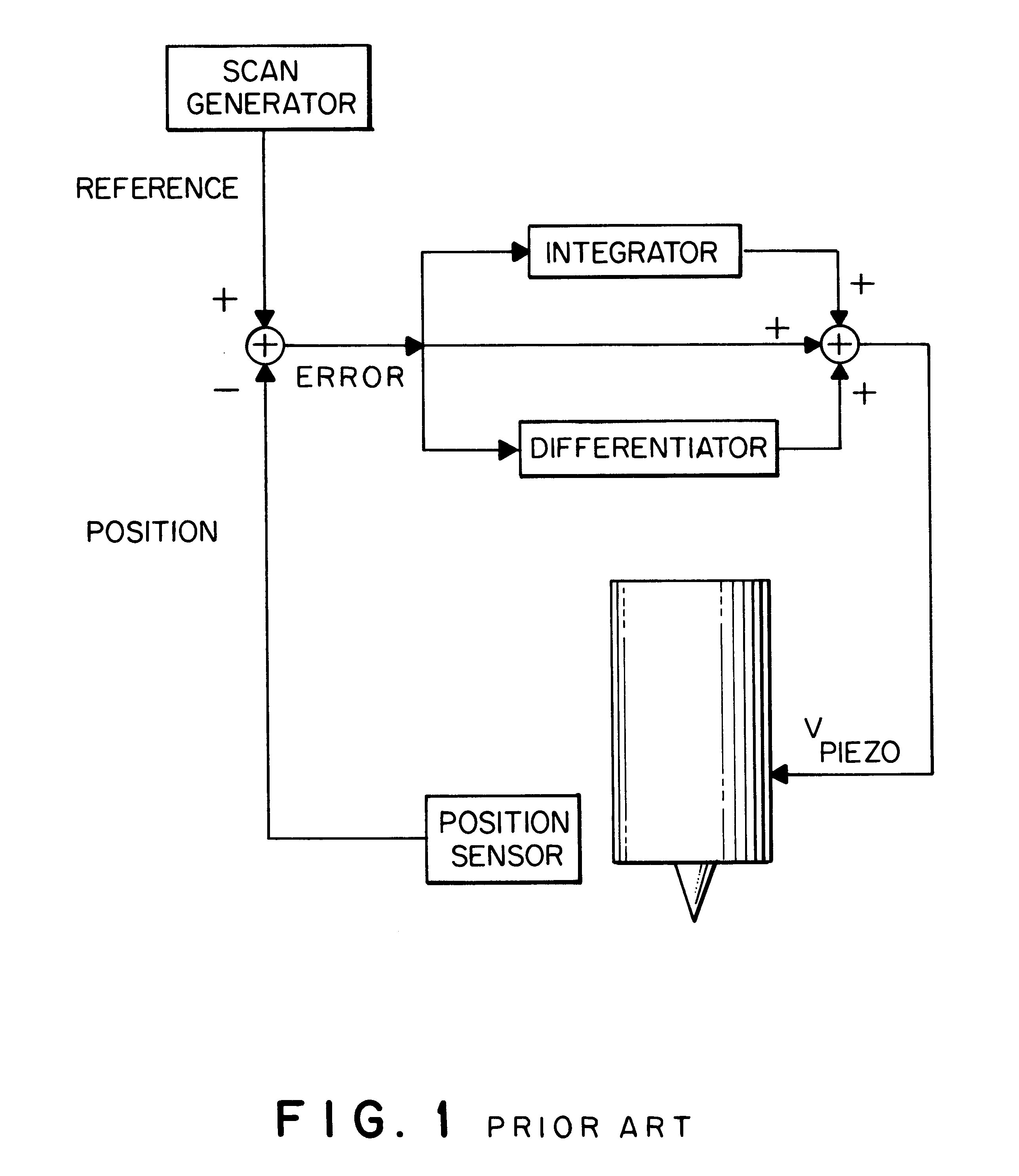
The prior art control methods which rely on integration of the error signal to achieve an accurate linear scan take longer to recover control after reversal since the transient error is stored by the integral.
The conventional closed loop control also fails to anticipate the special scan voltage requirements of piezoelectric transducers discussed by Elings et al in U.S. Pat. No. 5,051,644.
Unfortunately, it is difficult to find a sensor that matches well the operating dynamic range and bandwidth requirements of many piezoelectric scanners.
While position sensors used in the prior art work acceptably for large scale scans, most do not have sufficient resolution to control accurately scans on the nanometer scale.
Since atomic scale scans may be only 1 nm square, this resolution is clearly inadequate.
This limits either the speed or the accuracy with which the scanner can be moved.
Unfortunately for scanning probe microscopes, most users wish to speed up the scan for the small scans to reduce the effect of 1 / f noise in the probe detection electronics and to minimize the effect of mechanical drift and transducer creep.
So the requirements do not match the prior art approaches.
In the few cases where sensors can be optimized to provide subnanometer resolution, the sensors usually lack the dynamic range to also measure motions on the 100-micron scale.
Also, since the output is periodic, they have potentially infinite dynamic range (the sensor can measure infinitely large position shifts by counting an arbitrarily high number of periods).
Since scanning probe microscopes and other modern scanning systems require motions on a much smaller scale, it has been insufficient in the prior art to simply count successive periods.
These complex devices are very expensive and are not easily adapted to scanning systems such as scanning probe microscopes.
Such sensors can not be used directly in conventional control systems without some form of linearization.
Such undesirable crosstalk adds to the difficulty of conventional feedback control systems.
There are serious drawbacks to turning the feedback off.
First, there is no longer any control over the scan size.
This can make it difficult to localize and then "zoom in" on an object of interest in a scanning probe microscope.
Another disadvantage to turning the feedback off at small scans is that there is no longer any correction for "creep."
"Creep" and other forms of drift are perhaps the largest source of distortions at small scan sizes, so turning off the feedback altogether is an unattractive alternative.

Method used


Image

  • Scan control for scanning probe microscopes
  • Scan control for scanning probe microscopes
  • Scan control for scanning probe microscopes

Examples


Embodiment Construction

The invention is a method of controlling a scanner using a parametric scan voltage waveform whose parameters are updated using a motion sensor to sense plural scanner positions which are compared to the desired scanner motion and used to vary the scan voltage parameters to maintain the scan linear and free of drift and creep. The method implemented uses a high speed digital computer to process the position data according to a single numerical algorithm, or a set of related algorithms which share data in a digital memory, including the steps of: calculating the parameters of a position function describing the scanner motion, comparing the position function parameters with values set by the operator and stored in memory to obtain a measure of the error in the scan, and adjusting another set of parameters defining the scan voltage according to the measured scan error in order to cause the scanner to deflect linearly with time and to compensate for scanner drift and creep. This is in co...


PUM

PropertyMeasurementUnit
scan sizesaaaaaaaaaa
scan voltageaaaaaaaaaa
sizeaaaaaaaaaa

Abstract

A method of controlling a scanner, particularly a scanner for use in scanning probe microscopes such as an atomic force microscope, including the steps of generating a scan voltage which varies as a parametric function of time, applying the scan voltage to the scanner, sensing plural positions of the scanner upon application of the scan voltage, fitting a parametric function to the sensed scanner positions, and controlling at least one parameter of the scan voltage function based on the parametric function fitted to the sensed scanner positions in the fitting step. In a preferred embodiment, the scan voltage is a polynomial parametric function of time and the order of terms of the polynomial is set in relation to the size of the scan being controlled, with small scans having at least one order term and relatively larger scans having plural order terms. Thus, the sensed position data are used, not to control the motion of the scanner directly in a closed loop system, but instead to optimize the transducer calibration parameters for subsequent open looped scan control of a portion of a total scan, with the calibration of the transducer scan voltage parameters periodically occurring.

Description

BACKGROUND OF THE INVENTION1. Field of the InventionThis invention relates to the control of piezoelectric and other scanners, and more specifically to scan control for scanning probe microscopy and other fields requiring a precision scanning stage.2. Discussion of BackgroundPrecision scanning stages are required by disciplines including scanning probe microscopy, beam lithography, and others. A common form of scanner for these applications is the piezoelectric scanner. The piezoelectric scanner comes in a variety of forms--single crystals, bimorphs, multilayer piezoelectric stacks, and tube scanners, for example. For all of these configurations, a voltage is applied across the piezoelectric elements and the position of some part of the piezoelectric scanner moves with respect to another part that is held fixed. This motion is used to scan samples, probes, lenses, etc., for a variety of purposes. Such scanners are often used to produce motion of the probe over the sample. However, m...

Claims


Application Information

Patent Timeline
Patent Type & Authority Patents(United States)
IPC IPC(8): G01B7/00G12B21/20G12B21/00G12B21/08G12B21/02G01Q10/06G01Q20/04G01Q30/04G01Q40/00G01Q60/26G05D3/12
CPCB82Y35/00G01Q40/00G01B7/003Y10S977/851
Inventor ELINGS, VIRGIL B.
Owner BRUKER NANO INC
Learn More