Grating coupled vertical cavity optoelectronic devices

a vertical cavity optoelectronic and grating technology, applied in the direction of lasers, lasers, semiconductor lasers, etc., can solve the problems of large waveguide loss, limitation of modulation bandwidth, and inability to realize optical sources with those modulation bandwidths

Inactive Publication Date: 2005-01-04
UNIV OF CONNECTICUT
View PDF4 Cites 14 Cited by
  • Summary
  • Abstract
  • Description
  • Claims
  • Application Information

AI Technical Summary

Benefits of technology

The device is described in one illustrative embodiment of the HFET inversion channel laser, which comprises one of the laser devices in the general family of inversion channel optoelectronic devices which are modulation doped devices. In this form of the invention, a refractory metal emitter provides a conduction path of hole flow into the laser active region by two-dimensional conduction. The two dimensional contour of the conduction with path is established by an N type implant under the metal emitter. The refractory metal emitter is constituted of two metal stripes one positioned on either side of an optical waveguide which utilizes the upper D

Problems solved by technology

Realizing optical sources with those modulation bandwidths remains a significant obstacle however.
The limitations on this bandwidth arise from the non-linear gain mechanism and from the maximum values of differential gain that can be realized.
However, in the edge emitter these regions cannot be reduced to much less than about 1500 Å in thickness and yet still maintain a reasonable value for I′, the optical confinement factor for the quantum well in the optical waveguide.
Also, as the low index waveguide regions are placed closer to the quantum well, the large index difference interfaces produce larger waveguide loss.
This limit is imposed by the rapidly rising threshold current and the reduced power capability.
The larger threshold, of course, results in lower maximum power due to the reduced current range for optica

Method used


Image

  • Grating coupled vertical cavity optoelectronic devices
  • Grating coupled vertical cavity optoelectronic devices
  • Grating coupled vertical cavity optoelectronic devices

Examples


Embodiment Construction

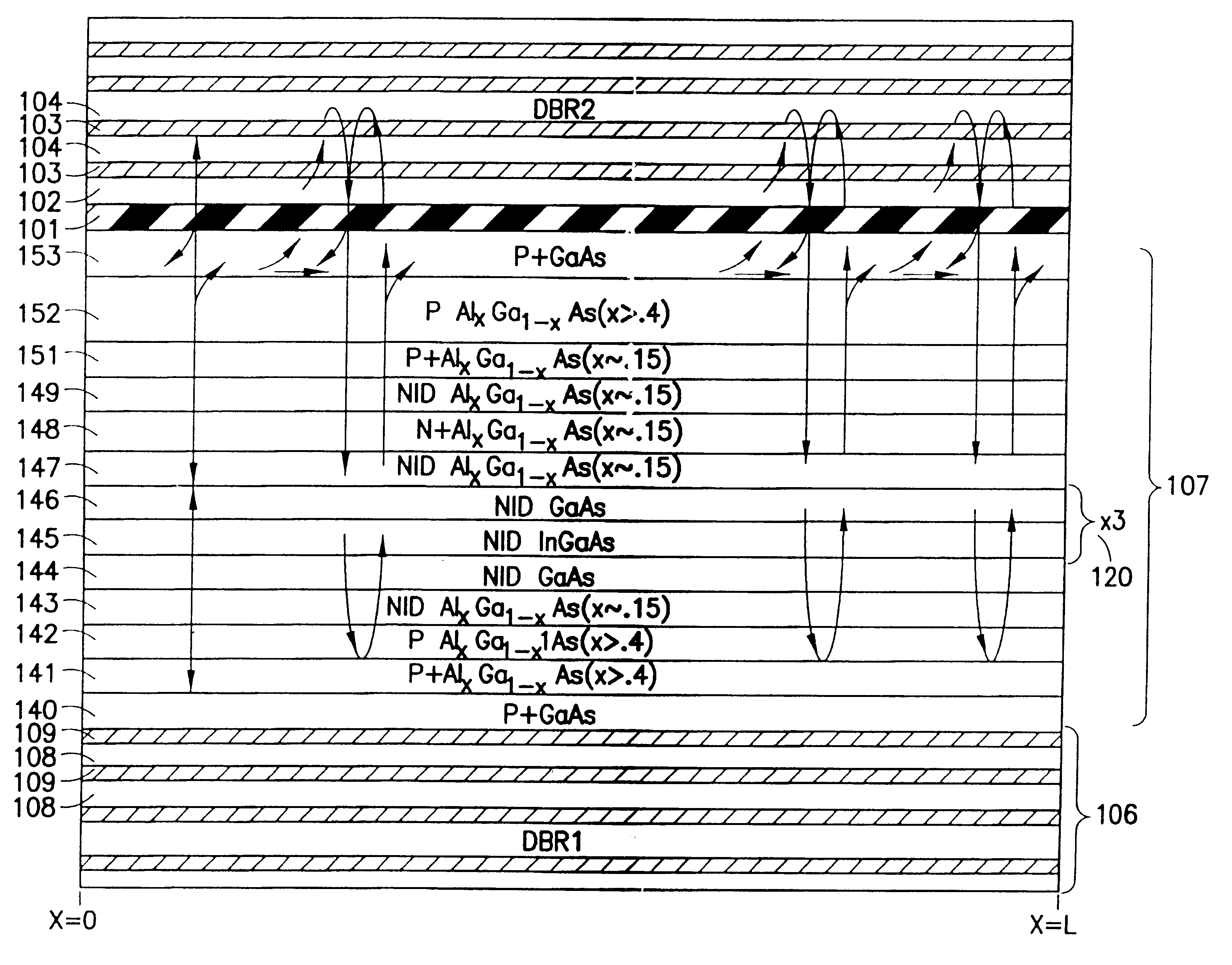
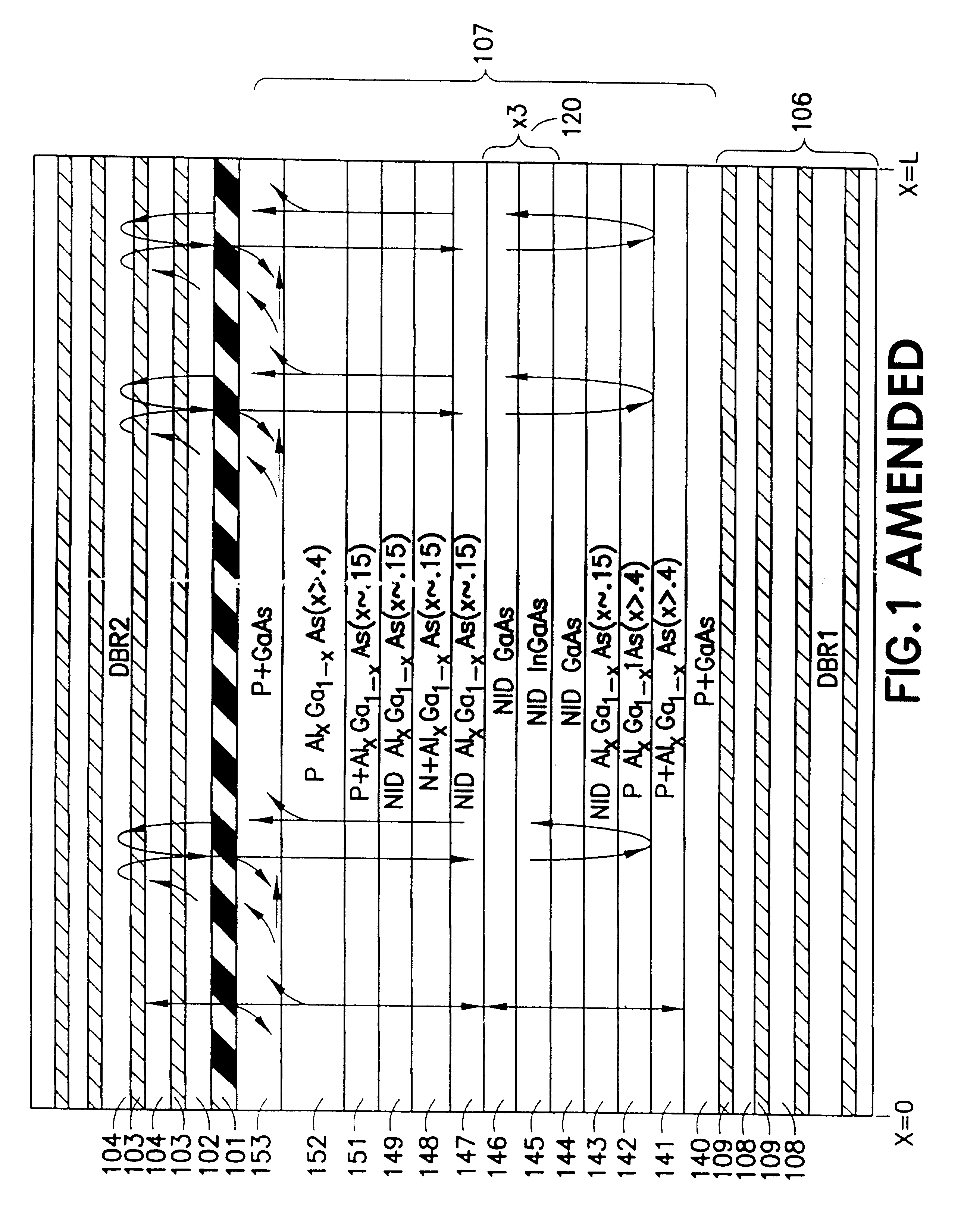
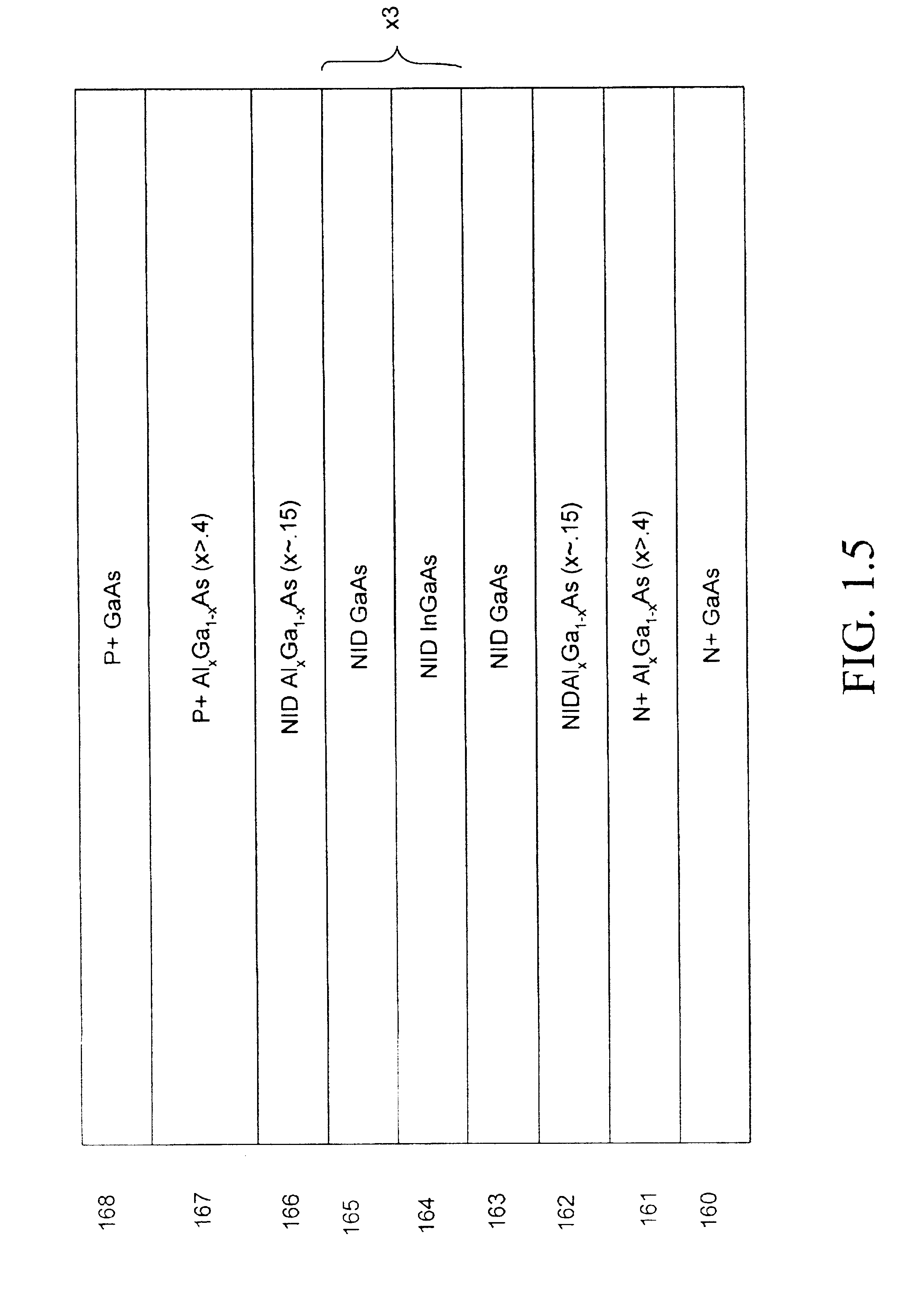
FIGS. 1,2,3 shows the layers of a structure in accordance with a preferred embodiment and from which all the devices of the invention can be made. The semiconductor layer structure and fabrication are in accordance with the Inversion Channel Technology and have been described in detail in application Ser. No. 60 / 028,576. A vertical cavity laser is constructed comprised of: a lower DBR mirror 106 consisting typically of alternating layers 108 of GaAs and 109 of AlAs which itself will be oxidized during the fabrication to form layers 109 of AlxOy, a active laser cavity 107 consisting of the standard SCH (separate confinement heterostructure) semiconductor laser structure containing say 3 quantum wells 120 which may be the laser structure of the inversion channel laser as discussed here or the conventional pn laser structure, a top DBR mirror consisting of alternating layers 101, 102, 103, and 104 of two deposited dielectrics. For the inversion channel laser this structure consists of ...


PUM


Abstract

A edge emitting waveguide laser is obtained that derives its optical power from a vertical cavity laser structure. The vertical cavity laser with top and bottom Distributed Bragg Reflectors produces stimulated emission by resonance in the vertical direction but the optical power so generated is diffracted by a second order grating into an optical mode propagating in the optical waveguide formed by the upper and lower mirrors as cladding layers. The efficiency of the diffraction grating and the reflectivity of the mirrors are maximized so that essentially all of the light is coupled into the guide and the loss through the mirrors can be neglected. The same structure can be utilized as a detector, a modulator or an amplifier. The designated laser structure to achieve this form of operation is the inversion channel laser which is a laterally injected laser having both contacts on the top side of the device. Then the anode and cathode of the laser are essentially coplanar electrodes and the device is implemented in the form of a traveling wave laser, detector, modulator or amplifier which forms the basis for very high frequency performance.

Description

TECHNICAL FIELD OF THE INVENTIONThis invention relates to the field of semiconductor double heterostructure laser devices and, in particular, to those laser devices which use vertical cavities. It also relates to the field of corrugated optical waveguides and travelling wave optoelectronic devices.BACKGROUND OF INVENTIONNext generation transmission systems are anticipating bit rates approaching 100 Gb / s in time division multiplexed architectures. The demand for such speeds is created by the growth of interactive multi-media services and is made possible by the terahertz bandwidth of optical fiber. Realizing optical sources with those modulation bandwidths remains a significant obstacle however. The state-of-the-art edge-emitting semiconductor lasers have 3 db bandwidths in the region of 30 GHz. The limitations on this bandwidth arise from the non-linear gain mechanism and from the maximum values of differential gain that can be realized. The non-linear gain effect is due to the pres...

Claims


Application Information

Patent Timeline
IPC IPC(8): H01S5/062H01S5/12H01S5/183
CPCH01S5/0424H01S5/06203H01S5/06226H01S5/12H01S5/18308H01S5/18341H01S5/18369H01S5/18372H01S5/2027H01S5/2275
Inventor TAYLOR, GEOFF W
Owner UNIV OF CONNECTICUT
Why Eureka
Try Eureka