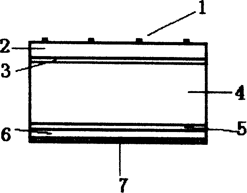
Tin dioxide thin film and silicon heterojunction solar battery
A tin dioxide and silicon heterojunction technology, applied in circuits, photovoltaic power generation, electrical components, etc., can solve the problems of low efficiency, the problem of passivation of the back electrode of the battery is not well solved, and the cost of indium oxide films is high. Achieve the effects of low industrialization cost, improved electrical output performance, and improved stability
- Summary
- Abstract
- Description
- Claims
- Application Information
AI Technical Summary
Problems solved by technology
Method used
Image
Examples
example
[0030] The n-type silicon substrate 4 selects n-type Czochralski monocrystalline silicon wafers with a resistivity of 1 Ωcm. The silicon wafers are (100) oriented, polished on one side, and have a thickness of 250 μm. The effective area of the solar cell obtained is 2×2 cm 2 , the thickness of the fluorine-doped tin dioxide layer 2 is 76nm, the thicknesses of the intrinsic amorphous silicon film 5 and the phosphorus-doped amorphous silicon film 6 are 3nm and 30nm respectively, and the thickness of the silicon dioxide layer 3 is 2nm. The performance test results of the battery are: AM1.5, 100mW / cm 2 Under the irradiation of standard light intensity, the efficiency of the heterojunction solar cell prepared by this process reaches 14.2%, the open circuit voltage reaches 590mV, the short circuit current reaches 36mA, and the fill factor reaches 67%.
PUM
 Abstract
Description
Claims
Application Information
