Back shining type ZnO base ultraviolet imaging solid state focal plane detection array and its preparation

A detection array and ultraviolet imaging technology, applied in semiconductor/solid-state device manufacturing, final product manufacturing, radiation control devices, etc., can solve problems such as poor radiation resistance, image quality degradation, and uneven spatial response of the array

Inactive Publication Date: 2009-11-18
XI AN JIAOTONG UNIV
View PDF4 Cites 6 Cited by
  • Summary
  • Abstract
  • Description
  • Claims
  • Application Information

AI Technical Summary

Problems solved by technology

In addition, the radiation resistance of CCD is very poor, which will not only cause a decline in image quality, but also affect the charge collection efficiency of the channel, resulting in uneven spatial response of the array

Method used


Image

  • Back shining type ZnO base ultraviolet imaging solid state focal plane detection array and its preparation
  • Back shining type ZnO base ultraviolet imaging solid state focal plane detection array and its preparation
  • Back shining type ZnO base ultraviolet imaging solid state focal plane detection array and its preparation

Examples


Embodiment Construction

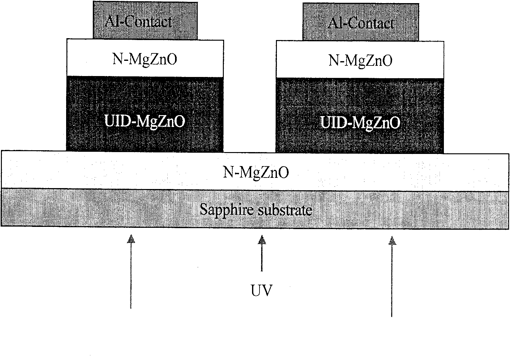
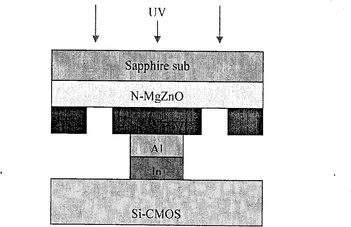
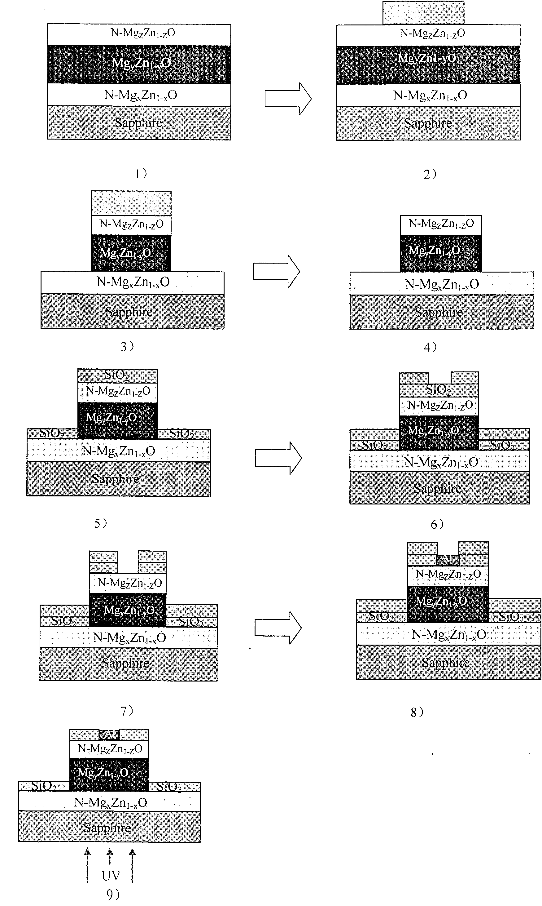
[0017] The invention realizes a back-illuminated ZnO-based ultraviolet imaging solid-state focal plane detection array and a preparation method thereof. The structure of each imaging unit is shown in the attachment figure 1 As shown, the production method is as follows image 3 shown.

[0018] The ultraviolet imaging detection array uses double-sided polished sapphire (0001) as a substrate, and Al heavily doped N- Mg x Zn 1-x O or Be x Zn 1-x The O layer is used as a transparent conductive film for the electrode and the UV-C light window layer to ensure that the light in the UV-C band is fully transmitted; and the N-Mg of this layer x Zn 1-x O or Be x Zn 1-x The x value of O should be as large as possible, so that its band gap is large, and the ultraviolet light absorption of UV-C is less, and this layer also determines the short-wavelength limit of the imaging device, (cut-on). Other conductive films transparent to the UV-C band can also be used.

[0019] Then epit...


PUM


Abstract

The invention relates to a backlight ZnO-based ultraviolet imaging solid focal plane surveying array and preparation, which on the sapphire (0001)substrate of double-face polishing, uses laser molecular beam to epitaxially grow a MgxZn1-xO(BexZn1-xO) nesa heavily doped with Al, then epitaxially growing a MgyZn1-yO layer without adulterant, sensitive to ultraviolet light. Then a MgzZn1-zO ohm contact epitaxial layer heavily doped with Al is gengerated on the upper surface. An array pixel cell structure is formed by using a photoetching and ICP ion etching method, then uses RF magnetron sputtering to plate a SiO2 passivation layer, based on the etched graph. An Al contact of electrodes etched by reactive ion uses a method of evaporation plated film to form a metallic contact, for rapid annealing activation of an ultraviolet sensitive active layer to form an ohm contact, thus getting a backlight ZnO-based ultraviolet imaging solid focal plane surveying array. The invention and the matched Si-CMOS readout circuit chip are interconnected through indium bumps, which are put on the focal plane of the ultraviolet lens, added with the corresponding image processing, memory circuit and software to form a complete ultraviolet imaging device.

Description

technical field [0001] The invention belongs to the field of photoelectric imaging, and relates to a structural design and a preparation method of a back-illuminated ZnO-based ultraviolet imaging solid-state focal plane detection array, which is a core component of a back-illuminated ZnO-based solid-state focal plane array ultraviolet imaging device. Background technique [0002] Ultraviolet imaging can be widely used in research fields such as astronomical observation, ultraviolet guidance and early warning, medical imaging, public security criminal investigation, non-visual short-distance secure communication, aerospace, environmental monitoring, biological species exploration and identification, etc. The application of ultraviolet band in space astronomical observation has developed ultraviolet astronomy. The main function of space ultraviolet observation is to study the stellar atmospheric model and interstellar matter through the detection of outer space ultraviolet rad...

Claims


Application Information

Patent Timeline
Patent Type & Authority Patents(China)
IPC IPC(8): H01L27/144H01L21/84H01L31/101H01L31/18
CPCY02P70/50
Inventor 张景文毕臻边旭明侯洵杨晓东韩峰
Owner XI AN JIAOTONG UNIV
Why Eureka
Try Eureka