Preprocessed chip of porous silica microfluid sample
A technology for porous silica and sample pretreatment, which is used in material testing products, chemical instruments and methods, and microbial determination/inspection. Effect
- Summary
- Abstract
- Description
- Claims
- Application Information
AI Technical Summary
Problems solved by technology
Method used
Image
Examples
Embodiment 1
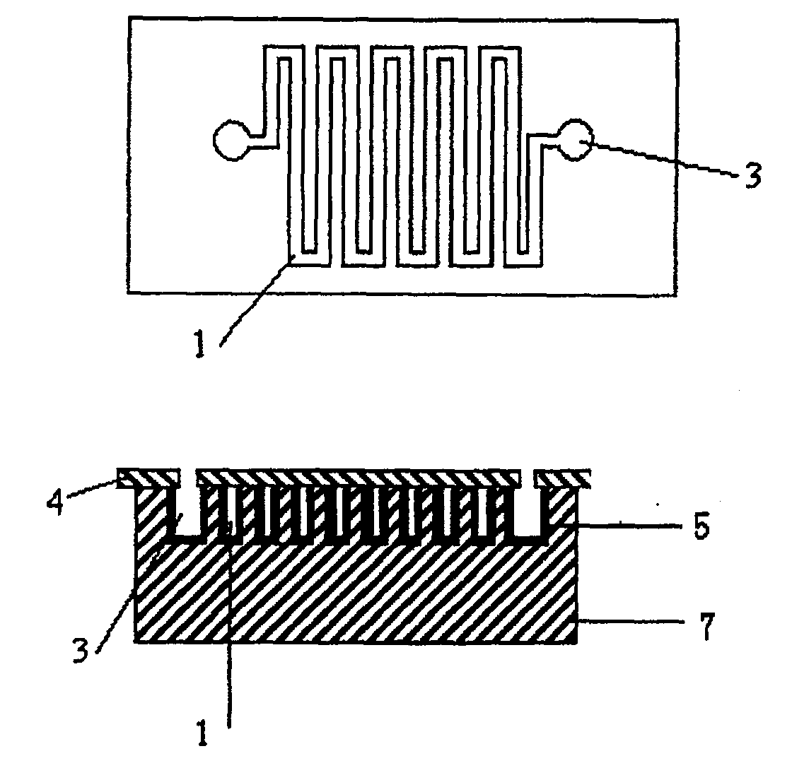
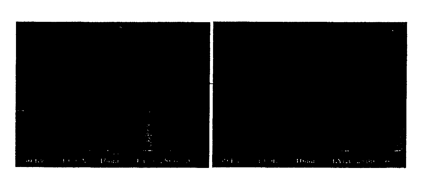
[0040] Clean N-type low resistance (0.011-0.014Ω.cm) double-sided polished single crystal silicon wafer 7; grow 2000 Silicon nitride (the thickness of silicon nitride can be selected from 1000-7000 ) as etching silicon wafer 7 and the mask of preparing porous silicon oxide; Get rid of negative photoresist BN303 (negative glue), develop after exposure on the Karlsuss MA4 type photolithography machine; Use SF on the plasma etching machine 6 Remove the silicon nitride; use KOH anisotropic etching solution to etch out the flow cell 3 with a depth of 120 μm, the flow cell 3 with a depth of 120 μm (the depth can be selected as 80-150 μm), and the microchannel 1 with a width of 200 μm, Sample injection and sample discharge flow cell 3 are blind holes with opening upwards; porous silicon is prepared by electrochemical corrosion in hydrofluoric acid (HF) ethanol solution (porous silicon is dendritic or spongy, such as image 3 Shown); 550 ℃ low-temperature thermal oxidation growth p...
Embodiment 2
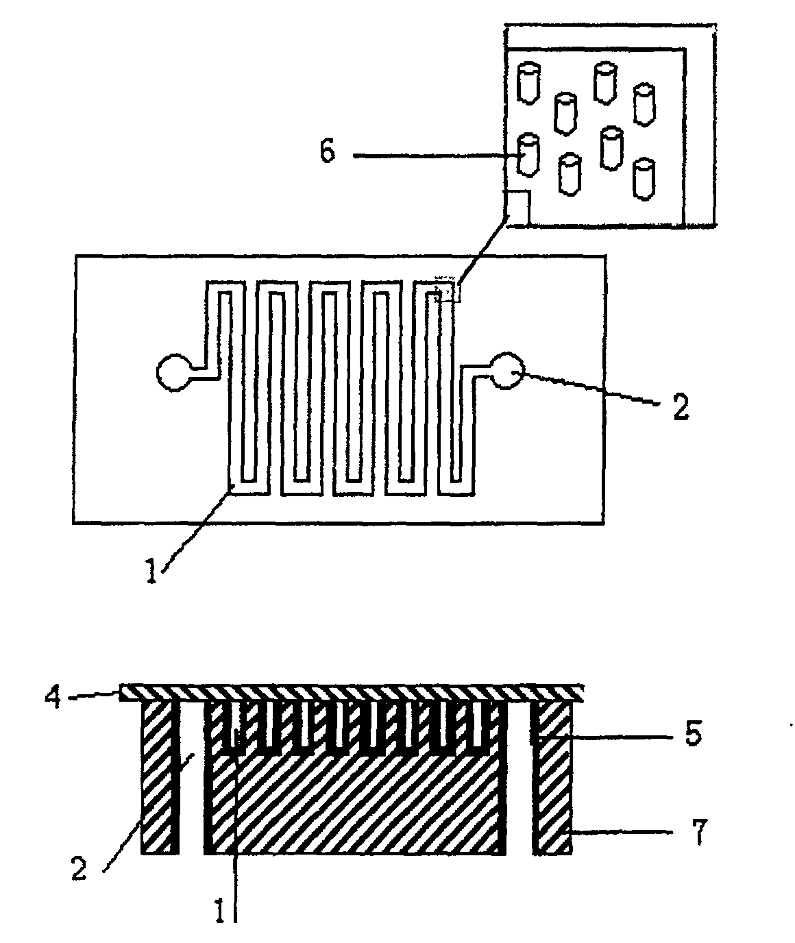
[0042] Clean N-type low resistance (0.011-0.014Ω.cm) double-sided polished single crystal silicon wafer 7; grow 2000 Silicon nitride (the thickness of silicon nitride can be selected from 1000-7000 ) as a mask for etching silicon wafer 7 and preparing porous silicon oxide; positive photoresist AZ1500 or AZ4620 (positive photoresist) is used as a photolithographic mask, and is developed after exposure on a Karlsuss MA4 photolithography machine; deep etching technology etching Sample inlet and outlet holes 2, sample inlet and outlet holes 2 are through holes on the monocrystalline silicon wafer; photoresist is removed with acetone; the second photolithography is developed after exposure on a Karlsuss MA4 photolithography machine; The deep etching technology etches the channel 1 with a depth of 80 μm (the depth can be selected as 80-200 μm) or the channel 1 with a depth of 80 μm (the depth can be selected as 80-200 μm) and the micro-column 6 in the channel (the gap between the ...
PUM
| Property | Measurement | Unit |
|---|---|---|
| height | aaaaa | aaaaa |
Abstract
Description
Claims
Application Information


