
Method for correcting layering optical proximity effect

A technology of optical proximity effect and correction method, which is applied in the direction of microlithography exposure equipment, special data processing application, photolithographic process exposure device, etc., can solve the problems of limited scope of application and limited performance improvement, and achieve the purpose of improving computing speed, Effects of speed improvement and cost reduction

Inactive Publication Date: 2007-08-08
ZHEJIANG UNIV
View PDF0 Cites 25 Cited by
  • Summary
  • Abstract
  • Description
  • Claims
  • Application Information

AI Technical Summary

Problems solved by technology

However, although the accuracy of the results of this method is satisfactory, its scope of application is very limited. The area of ​​completely consistent graphics in the layout is not large. If only the area within a certain range of them can save redundant operations, then the performance The improvement is very limited, so at present this method is mainly used in the processing of RAM layout with a large number of repeated graphics

Method used


Image

  • Method for correcting layering optical proximity effect
  • Method for correcting layering optical proximity effect

Examples


Embodiment Construction

[0037] Further illustrate the present invention below in conjunction with accompanying drawing.

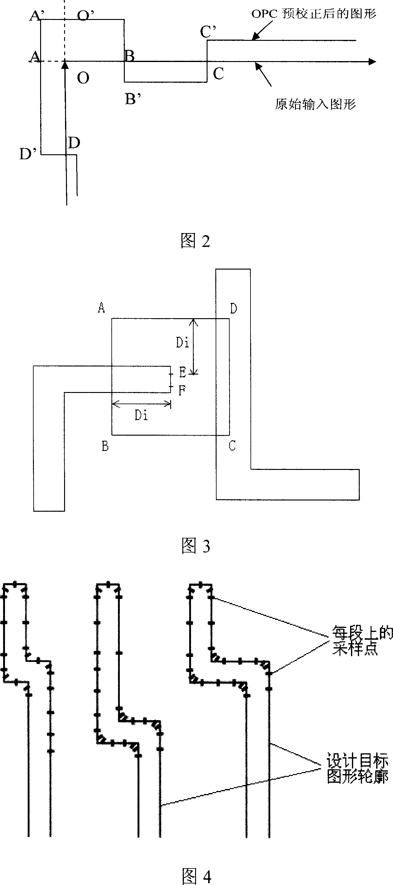
[0038] The hierarchical optical proximity effect correction method, the process is shown in Figure 1, including the preparation of the pre-correction cell library (Post-OPC Cell Library), the initialization of the mask pattern offset and the fast calculation using the dynamic adjustment algorithm, the steps are as follows :

[0039] 1) Initialization:

[0040] Set the simulation model for optical proximity effect correction (Simulation Model),

[0041] Photolithographic mask pattern, GDSII input,

[0042] The basic parameters of the lithography machine, λ, NA, σ,

[0043] where λ is the wavelength of the light source, NA is the numerical aperture of the optical system, and σ is the coherence coefficient of the illumination;

[0044] 2) Prepare the pre-calibration cell library:

[0045] Before the formal operation, the traditional model-based optical proximity effect correctio...


PUM


Abstract

The invention discloses a hierarchical optical proximity effect correction method, including the preparation of the pre-correction module library, the initialization of the mask graphic offset and the step using dynamic adjustment algorithm for rapid computation, and it provides a method to make full use of the territory hierarchical structure in the optical proximity effect correction, and under the deep submicron conditions, the high precision mask process is considered as high costs for too big calculation quantities, and the computational complexity can be greatly reduced under the help of the new algorithm, and meanwhile, the new approach provides the module library with pre-correction results to IC design process, making the design engineer more flexible and effective to check the design. The method of the invention can be used for aided high-precision IC mask board, to increase the results predictability in IC design process, and OPC correction computational speed, lower costs, and increase IC production yield and reduce production cycle.

Description

technical field [0001] The invention relates to a layered optical proximity effect correction method, which is suitable for assisting in the manufacture of high-precision integrated circuit reticles and belongs to the field of integrated circuit computer aided design. Background technique [0002] When the minimum feature size and spacing of integrated circuits are reduced below the wavelength of the light source used in lithography, due to the inevitable effects of light diffraction and photoresist development and etching, the mask (Mask) pattern and silicon The graphics printed on the wafer will no longer be consistent, and the distortion of IC layout graphics transfer will increase significantly, seriously affecting the production yield of integrated circuits. This phenomenon is called "Optical Proximity Effect (OPE, Optical Proximity Effects)". Usually, the distortion phenomenon produced by the graphics actually printed on the silicon wafer includes: corner rounding or ...

Claims


Application Information

Patent Timeline
Patent Type & Authority Applications(China)
IPC IPC(8): G03F7/20G06F17/50H01L21/027H01L21/00
Inventor 严晓浪史峥张宇孚
Owner ZHEJIANG UNIV
Learn More