White light GaN LED epitaxial material without fluorescent powder conversion and method for making the same

A technology for light-emitting diodes and epitaxial materials, which is applied in electrical components, circuits, semiconductor devices, etc., can solve the problems of lack of UV radiation resistance, limited light-emitting quality of white light-emitting diodes, low light-emitting efficiency, etc., and achieves increased device complexity. The effect of improving light utilization efficiency and simplifying the production process

Inactive Publication Date: 2007-09-19
INST OF PHYSICS - CHINESE ACAD OF SCI
View PDF0 Cites 36 Cited by
  • Summary
  • Abstract
  • Description
  • Claims
  • Application Information

AI Technical Summary

Problems solved by technology

Among them, method (1) has not been applied due to cost and technical reasons; method (2) is a relatively simple and most promising white light-emitting diode manufacturing method, but has not yet found a suitable ultraviolet radiation resistance The encapsulating resin and the lack of efficient red phosphors have not been widely used; method (3) is a commercialized white light emitting diode manufacturing method at present, and the luminescence of white light emitting diodes is also caused by the lack of suitable red phosphors. The quality is limited, the white light spectrum ob

Method used


Image

  • White light GaN LED epitaxial material without fluorescent powder conversion and method for making the same
  • White light GaN LED epitaxial material without fluorescent powder conversion and method for making the same
  • White light GaN LED epitaxial material without fluorescent powder conversion and method for making the same

Examples


Embodiment 1

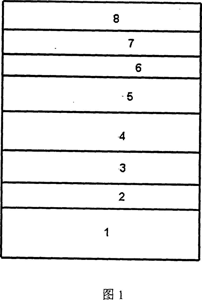
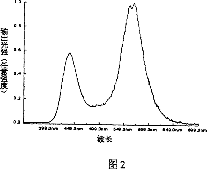
[0035] Using the method of the present invention and the white light GaN light-emitting diode epitaxy material of the present invention that does not require phosphor powder conversion to prepare a GaN single-tube-core white light light-emitting diode that does not require phosphor powder conversion, the steps are as follows:

[0036] 1) Using 0.43mm thick sapphire as the substrate 1, the GaN initial growth layer 2, the intrinsic GaN layer 3 (composed of GaN), and the 500nm thick n Type GaN layer 4 (composed of GaN), 1 μm thick InGaN relaxation layer 5 (composed of In 0.1 Ga 0.9 N composition), InGaN multi-quantum structure light-emitting layer 6 (composed of barrier layer In 0.05 Ga 0.95 N and quantum well layer In 0.15 Ga 0.85 5 periods of multiple quantum wells composed of N, in which the barrier layer In 0.05 Ga 0.95 The thickness of N is 10nm, the quantum well layer In 0.15 Ga 0.85 The thickness of N is 3nm, the barrier layer In y Ga 1-y The doping concentration...

Embodiment 2

[0042] Using the method of the present invention to prepare white light GaN light-emitting diode epitaxial materials that do not require phosphor powder conversion, the steps are as follows:

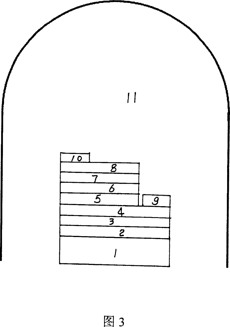
[0043] SiC with a thickness of 0.4 mm is used as the substrate 1, and an initial GaN growth layer 2, an intrinsic GaN layer 3 (composed of AlN), and n-type AlN with a thickness of 1 μm are sequentially grown on it by metal-organic chemical vapor deposition (MOCVD) Layer 4 (composed of GaN), 500nm thick InGaN relaxation layer 5 (composed of GaN), InGaN multi-quantum structure light-emitting layer 6 (composed of barrier layer GaN and quantum well layer In 0.15 Ga 0.85 4 periods of multiple quantum wells composed of N, in which the thickness of the barrier layer GaN is 12nm, and the quantum well layer In 0.15 Ga 0.85 The thickness of N is 5nm, the barrier layer In y Ga 1-y The doping concentration of N is 1×10 18 / cm 3 0, quantum well layer In x Ga 1-x The doping concentration of th...

Embodiment 3

[0045] Using the method of the present invention to prepare white light GaN light-emitting diode epitaxial materials that do not require phosphor powder conversion, the steps are as follows:

[0046] A 0.3 mm thick silicon substrate is used as the substrate 1, and a 200 nm thick AlN initial growth layer 2, a 1 μm thick intrinsic GaN layer 3 (composed of InGaN), 0.5 μm thick n-type GaN layer 4 (made of AlGaN), 10 nm thick InGaN relaxation layer 5 (made of In 0.2 Ga 0.8 N composition), InGaN multi-quantum structure light-emitting layer 6 (composed of barrier layer GaN and quantum well layer In 0.15 Ga 0.85 4 periods of multiple quantum wells composed of N, in which the thickness of the barrier layer GaN is 12nm, and the quantum well layer In 0.15 Ga 0.85 The thickness of N is 5nm, the barrier layer In y Ga 1-y The doping concentration of N is 1×10 17 / cm 3 , the quantum well layer In x Ga 1-x The doping concentration of the N layer is 2×10 17 / cm 3 ), 0nm thick p-typ...


PUM

PropertyMeasurementUnit
Thicknessaaaaaaaaaa
Thicknessaaaaaaaaaa
Thicknessaaaaaaaaaa

Abstract

The invention relates to epitaxial material of white light GaN light emitting diode which requires no phosphor for conversion and manufacturing method thereof, i.e. employing conventional semiconductor device deposition technique to orderly deposit an initial growth layer, an intrinsic GaN buffer layer, a n-type GaN layer, a InGaN relaxation layer, an InGaN luminescent layer of multi quantum structure, a p-type AlGaN interlayer and a p-type GaN layer; and employing the epitaxial material to make single chip white light light emitting diode; the method preserves the manufacturing techniques for making current normal monochromatic light light emitting diode device, and only improves the growth process of the GaN based luminescent material, thus, the In component achieves the level to form In quantum dot, and a stress releasing layer is added. In this manner, in the precondition of not increasing the complexity of the device, the production cost for making white light light emitting diode can be basically reduced, and the light emitting efficiency and utilization can be increased, and the weakness of the white light light emitting diode which employs phosphor for conversion can be overcome, and the whole performance of white light light emitting diode can be improved.

Description

technical field [0001] The invention relates to a white light emitting diode epitaxial material and a preparation method thereof, in particular to an epitaxial material and a preparation method for a white light GaN light emitting diode chip that does not require phosphor powder conversion. Background technique [0002] As a white light source, white light-emitting diodes have many advantages such as high luminous efficiency, short response time, and long life. These advantages determine that it will partially replace the existing white light source. At present, there are three kinds of manufacturing methods for white light-emitting diodes that are generally accepted: (1) three red, green and blue light-emitting diodes that are separately produced or integrated in a single chip emit light at the same time, thereby mixing white light, (2) The red, green and blue three-color mixed phosphor powder wrapped in the outer layer is excited by the ultraviolet or purple light-emitting...

Claims


Application Information

Patent Timeline
IPC IPC(8): H01L33/00H01L33/04
Inventor 陈弘贾海强郭丽伟周均铭王晓晖汪洋裴晓将
Owner INST OF PHYSICS - CHINESE ACAD OF SCI
Why Eureka
Try Eureka