Plasma treating apparatus and plasma treating method

A plasma and processing device technology, applied in the field of ion plasma processing devices, can solve problems such as insufficient countermeasures, and achieve the effect of improving etching speed and etching effect

Active Publication Date: 2007-09-26
TOKYO ELECTRON LTD
View PDF3 Cites 18 Cited by
  • Summary
  • Abstract
  • Description
  • Claims
  • Application Information

AI Technical Summary

Problems solved by technology

[0004] However, the technology disclosed in JP-A No. 10-4083, which covers metal oxides of group IIIB elements of the periodic table, exhibits relatively good plasma corrosion resistance, but in a more severe corrosive atmosphere gas , In the field of semiconductor processing technology in recent years, which requires high-precision processing and environmental cleanliness, it is not actually a sufficient countermeasure
[0005] In addition, disclosed in ...

Method used


Image

  • Plasma treating apparatus and plasma treating method
  • Plasma treating apparatus and plasma treating method
  • Plasma treating apparatus and plasma treating method

Examples


Embodiment 1

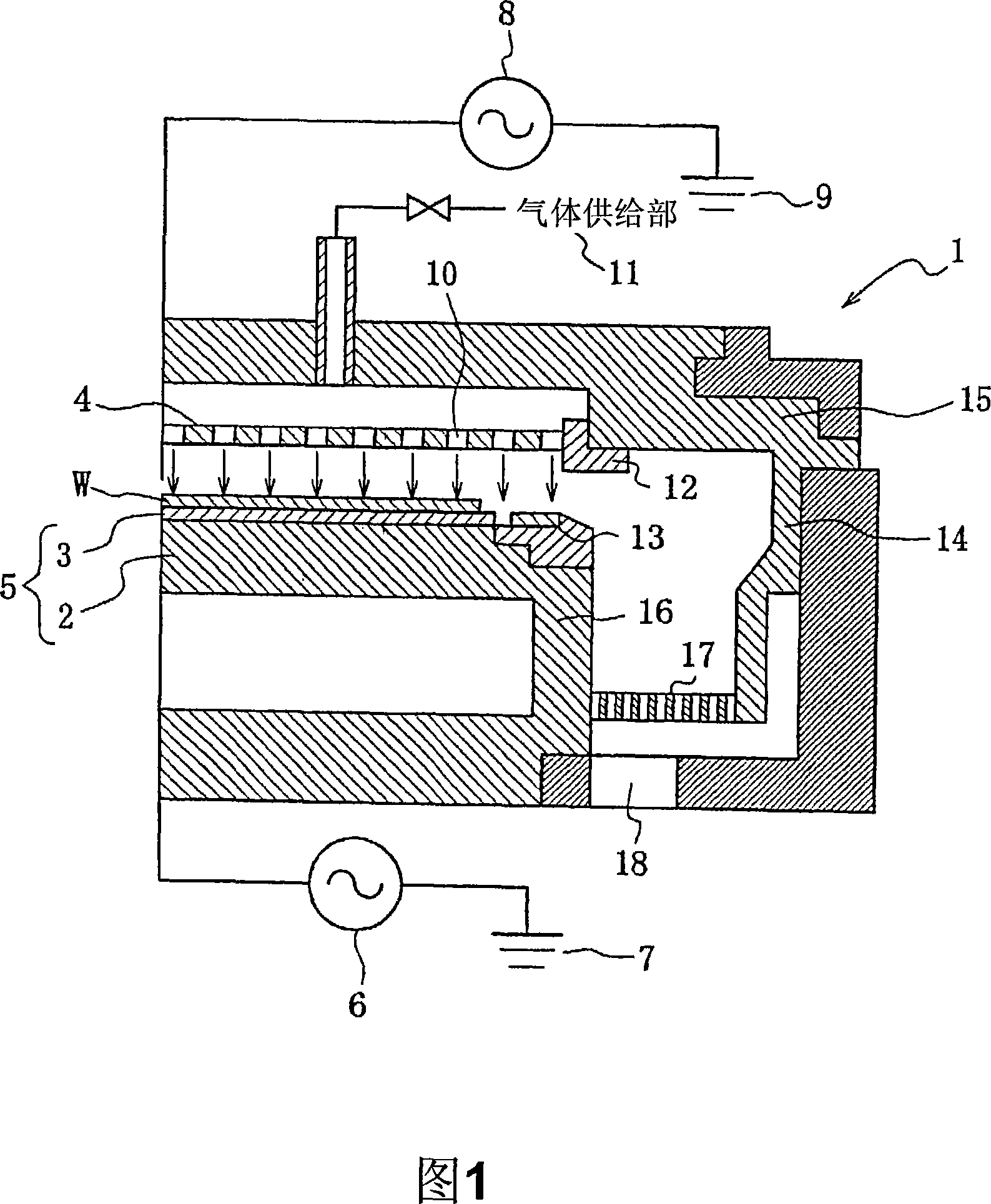
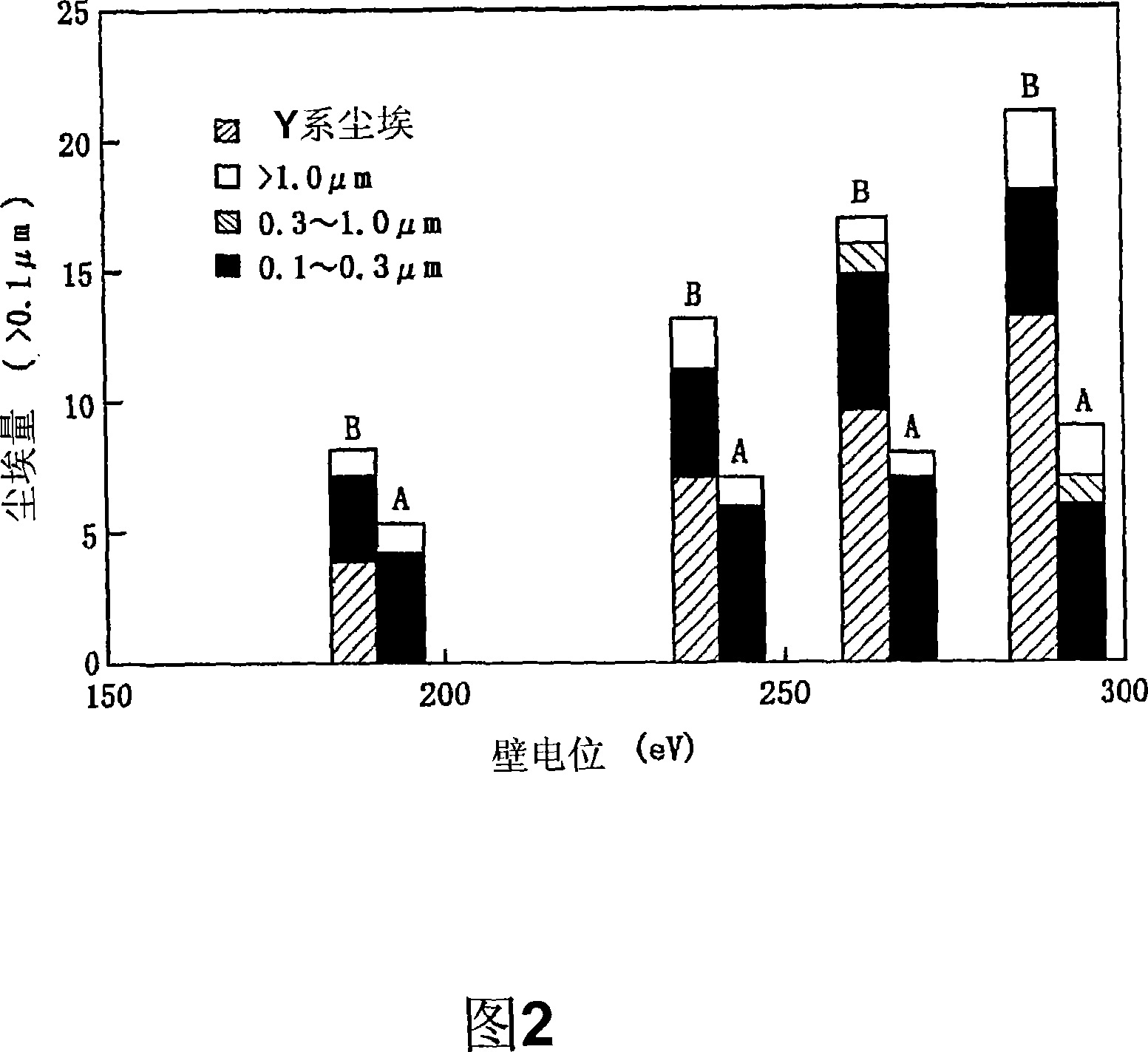
[0105] On the surface of the chamber inner wall member (aluminum baffle) of the plasma processing apparatus shown in FIG. 1, Y 2 o 3 (purity is more than 95mass%), obtains the part (comparative example B) that is formed with film; 2 o 3 After forming the film, the surface was irradiated with electron beams to undergo secondary transformation to form a member having a secondary crystal layer (invention example A). In each chamber, F-containing gas and CH-containing gas are alternately and repeatedly introduced, and plasma treatment is performed to make the above Y 2 o 3 After the sprayed coating is weakened, by controlling the amount of high-frequency power applied to the mounting table of the semiconductor wafer as the object to be plasma processed, the potential difference between the chamber wall potential and the plasma is changed from 200V to 300V, and each potential difference is measured. The amount of dust (particles) generated under the semiconductor wafer. The re...

Embodiment 2

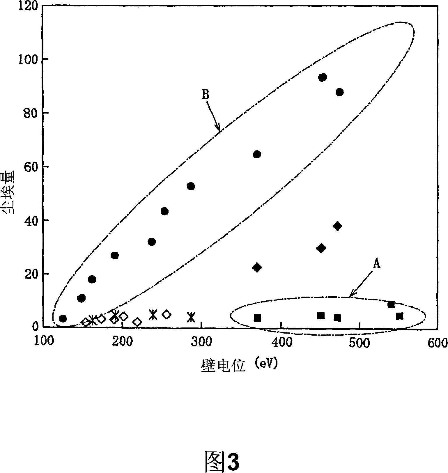
[0108] In order to investigate the limit value of the potential difference between the inner wall parts of the plasma processing container (aluminum lower insulator, baffle plate, deposit shield) and the plasma (the range that can suppress the generation of dust caused by the film (yttrium)), and Embodiment 1 prepares in the same way: on the surface of processing container inner wall parts, spray Y 2 o 3 And form the part (comparative example B) that has film; And in spraying Y 2 o 3 After the film was formed, the surface was irradiated with electron beams to undergo secondary transformation to form a component with a secondary crystal layer (invention example A). In each processing container, F-containing gas and CH-containing gas are introduced alternately and repeatedly for plasma treatment, so that Y 2 o 3 After the film was weakened, the amount of high-frequency power applied to the lower electrode was controlled to change the potential difference between the componen...


PUM


Abstract

Provided is a plasma processing apparatus wherein durability of a part, a member and a component, which are exposed to plasma atmosphere in a chamber used for performing plasma etching in a corrosion resistant gas atmosphere is improved, resistance to plasma erosion of a film formed on the surface of the member and the like in the corrosion resistant gas atmosphere is improved, and furthermore, generation of particles of corrosion resistant products even under high plasma output is prevented. A plasma processing method using such plasma processing apparatus is also provided. In the plasma processing apparatus for processing the surface of a subject which is stored in the chamber to be processed is processed by etching process gas plasma. The part exposed to the plasma generating atmosphere in the chamber or the member arranged inside the chamber or the surface of the component is coated with at least a porous layer composed of a metal oxide and a secondary recrystallized layer of the metal oxide formed on the porous layer.

Description

technical field [0001] The invention relates to a plasma processing device and a plasma processing method used in the technical field of semiconductor processing. In particular, it relates to the combination of halogen gas, inert gas, oxygen or hydrogen atmosphere, gas containing fluorine and fluorine compounds (hereinafter referred to as "F-containing gas") and hydrocarbon gas (hereinafter referred to as "CH-containing gas") A plasma processing apparatus and a plasma processing method for performing plasma etching processing, etc. on a semiconductor element, etc., in an environment constituted by an atmosphere or the like, or in an environment in which these atmospheres are formed alternately and repeatedly. Background technique [0002] When processing devices used in the semiconductor and liquid crystal fields, the plasma energy of a highly corrosive halogen-based etching gas is mostly used. For example, in a plasma etching treatment (processing) apparatus as one of semi...

Claims


Application Information

Patent Timeline
IPC IPC(8): H01L21/00H01L21/67H01L21/3065H01L21/311H01L21/3213C23F4/00H01J37/32B01J19/02
CPCC23C4/105C23C28/042C23C4/18C23C4/02C23C26/00H01J37/32495C23C4/11H01L21/3065
Inventor 小林义之
Owner TOKYO ELECTRON LTD
Why Eureka
Try Eureka