Novel electroluminescent device and method for producing the same

An electroluminescent device, an organic technology, applied in the direction of electrical solid-state devices, semiconductor/solid-state device manufacturing, electrical components, etc., can solve problems such as difficult to repeat device performance, high manufacturing costs, and applicability, and achieve light weight, chemical The effect of mature technology and fast response

Inactive Publication Date: 2008-01-30
UNIV OF ELECTRONIC SCI & TECH OF CHINA
View PDF0 Cites 12 Cited by
  • Summary
  • Abstract
  • Description
  • Claims
  • Application Information

AI Technical Summary

Problems solved by technology

At present, the complex device structure and manufacturing process have seriously affected its industrialization,

Method used


Image

  • Novel electroluminescent device and method for producing the same
  • Novel electroluminescent device and method for producing the same
  • Novel electroluminescent device and method for producing the same

Examples


Embodiment 1

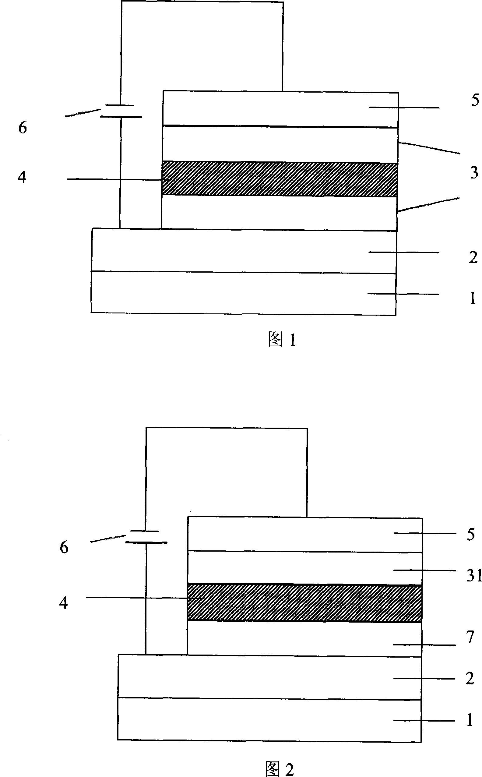
[0062] As shown in FIG. 2 , the light-emitting layer 3 in the structure of the device includes a blue light-emitting layer 31 , an electron transport layer 7 , and a compound control layer 4 . Devices that do not include the compound control layer 4 are conventional devices.

[0063] The material of the blue light-emitting layer of the device is NPB, and the material of the electron transport layer is Alq 3 , Composite control layer BCP, cathode layer with Mg:Ag alloy. The entire device structure is described as:

[0064] Glass substrate / ITO / NPB(20nm) / BCP(0nm or 0.3nm) / Alq 3 (50nm) / Mg:Ag(200nm)

[0065] The preparation method is as follows:

[0066] ①Use detergent, ethanol solution, acetone solution and deionized water to ultrasonically clean the conductive substrate ITO glass, and dry it with dry nitrogen after cleaning. Wherein the ITO film on the glass substrate is used as the anode layer of the device, the square resistance of the ITO film is 10Ω / □, and the film thickn...

Embodiment 2

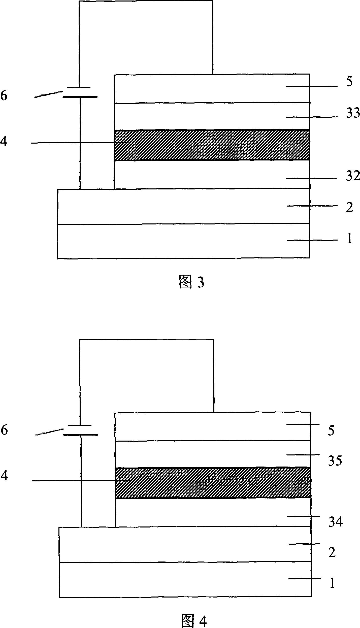
[0074] As shown in FIG. 3 , the light-emitting layer 3 in the structure of the device includes a blue light-emitting layer 32 , a green light-emitting layer 33 , and a composite control layer 4 .

[0075] The material of the blue light-emitting layer of the device is NPB, and the material of the green light-emitting layer is Alq 3 , Composite control layer BCP, cathode layer with Mg:Ag alloy. The entire device structure is described as:

[0076] Glass substrate / ITO / NPB(20nm) / BCP(1.5nm) / Alq 3 (50nm) / Mg:Ag(200nm)

[0077] The fabrication process of the device is similar to that of Example 1.

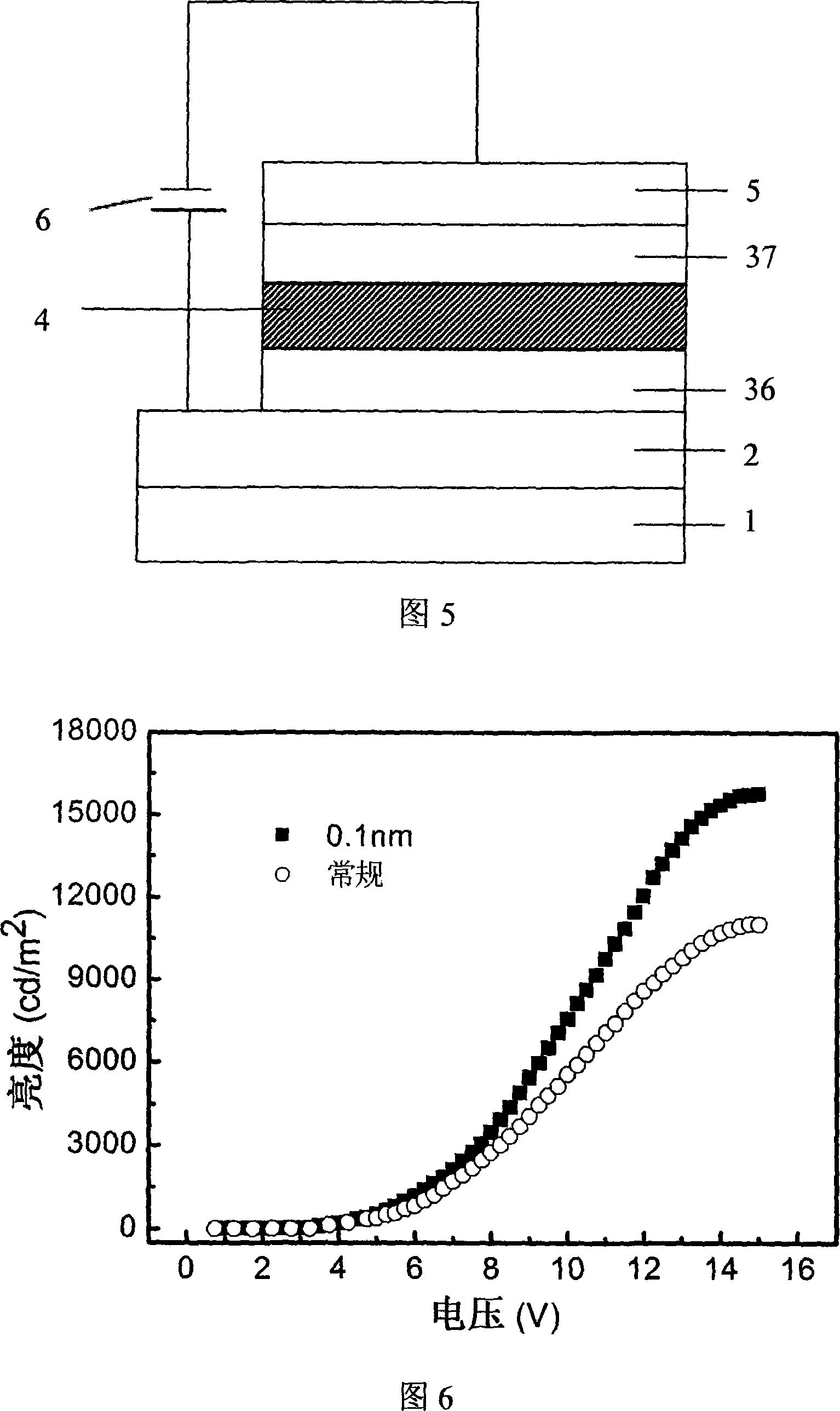
[0078] The luminescence spectrum of the device at a forward voltage of 10V is shown in FIG. 7 .

Embodiment 3

[0080] As shown in FIG. 4 , the light-emitting layer 3 in the structure of the device includes a blue light-emitting layer 34 , a red light-emitting layer 35 and a composite control layer 4 .

[0081] The material of the blue light-emitting layer of the device is NPB, and the material of the red light-emitting layer is Alq 3 : DCJTB, composite control layer BCP, cathode layer with Mg:Ag alloy. The entire device structure is described as:

[0082] Glass substrate / ITO / NPB(20nm) / BCP(0.3nm) / Alq 3 :DCJTB(50nm) / Mg:Ag(200nm)

[0083] The fabrication process of the device is similar to that of Example 1.


PUM

PropertyMeasurementUnit
Sheet resistanceaaaaaaaaaa
Film thicknessaaaaaaaaaa

Abstract

The invention discloses a novel organic electroluminescent device, comprising a conducting base plate or a substrate, an anode layer and a cathode layer, an electrode on the surface of the substrate or the conducting base plate and an organic functional layer between the anode layer and the cathode layer which comprises at least a luminescent layer emitting light driven by an additional power, and is characterized in that the organic functional layer further comprises one or more type of a compound regulation layer, an electron transporting layer, a hole-transporting layer and a hole blocking layer, the compound regulation layer is a carrier compound regulation layer which is made by one or more materials of poly-N-vinylcarbazole, BCP, two(2-methyl-8-quinoline acid radical complex)three phenyl silanol aluminum(III), two (2-methyl-8-quinoline acid radical complex)4-phenol aluminum(III) and two(2-methyl-8-quinoline acid radical complex)4-phenyl-based phenol aluminum (III).

Description

technical field [0001] The invention relates to the technical field of organic electroluminescence in electronic components, and relates to an organic electroluminescence device with a novel structure and a preparation method thereof. Background technique [0002] Organic electroluminescent displays have significant advantages: self-luminescence, low-voltage DC drive, high and low temperature resistance, full curing, wide viewing angle, rich colors, no need for backlight, large viewing angle, low power, and a response speed of up to 1000 times that of liquid crystal displays. times, while its manufacturing cost is lower than that of liquid crystal displays of the same performance, and it can provide technical support for micro-displays. Therefore, organic electroluminescence display has become a research hotspot. [0003] In 1987, C.W.Tang and others from the American Kodak Company invented a sandwich structure device on the basis of summarizing their predecessors: they use...

Claims


Application Information

Patent Timeline
IPC IPC(8): H01L51/50H01L51/54H01L51/56
Inventor 于军胜蒋亚东李璐唐晓庆李青
Owner UNIV OF ELECTRONIC SCI & TECH OF CHINA
Why Eureka
Try Eureka