Gallium nitride radical heterojunction field effect transistor structure and method for making the same

A heterojunction field effect, gallium nitride-based technology, applied in semiconductor/solid-state device manufacturing, semiconductor devices, electrical components, etc., can solve problems such as increased deep-level defects, reduced mobility, and increased interface roughness. Achieve the effects of improving the two-dimensional electron gas mobility, improving the crystal quality, and reducing the defect density

Inactive Publication Date: 2008-03-12
INST OF SEMICONDUCTORS - CHINESE ACAD OF SCI
View PDF0 Cites 22 Cited by
  • Summary
  • Abstract
  • Description
  • Claims
  • Application Information

AI Technical Summary

Problems solved by technology

However, doping will reduce the integrity of the material lattice, resulting in a decrease in the crystal quality of the AlGaN layer, and an increase in the roughness of the interface between the GaN and AlGaN layers, so the effect of improving the mobility is not ideal; (2) Using a high Al composition barrier layer AlGaN/GaN HEMT structure, as the Al composition of the barrier layer increases, the heterojunction band order and polarization electric field increase, which can significantly increase the two-dimensional electron gas concentration
However, when the Al composition is high, the large lattice mismatch will lead to the deterioration of the crystal quality, surface and interface quality of the AlGaN barrier l

Method used


Image

  • Gallium nitride radical heterojunction field effect transistor structure and method for making the same
  • Gallium nitride radical heterojunction field effect transistor structure and method for making the same
  • Gallium nitride radical heterojunction field effect transistor structure and method for making the same

Examples


Embodiment Construction

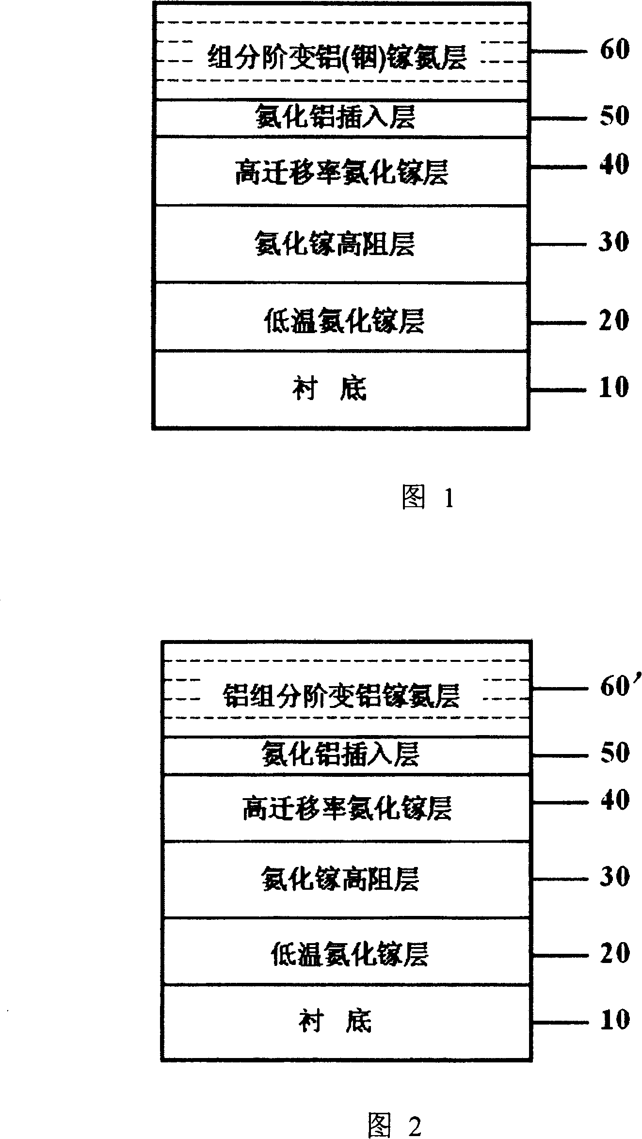
[0060] The key of the present invention is that the structure adopts a unique composition step change aluminum (indium) gallium nitrogen barrier layer structure (along the growth direction, the energy band level changes from high to low, and maintains a large energy band at the heterojunction interface. The band step is discontinuous, and then the energy band step gradually decreases to the surface of the barrier layer), a new type of high-mobility gallium nitride thin layer is used as the channel layer, and the gallium nitride channel layer and aluminum (indium) gallium nitride A thin layer of aluminum nitride insertion layer is introduced between the barrier layers. By precisely controlling the growth conditions, such as temperature, pressure, and V / III ratio, the stress caused by lattice mismatch and thermal expansion mismatch is effectively relieved, and the nitrogen The defect density of the GaN epitaxial layer improves the crystal quality of the channel layer, and the GaN...


PUM

PropertyMeasurementUnit
Thicknessaaaaaaaaaa
Thicknessaaaaaaaaaa
Room temperature resistivityaaaaaaaaaa

Abstract

The invention is a GaN-based HFET structure, which comprises an underlay, a low-temperature GaN nucleating layer which is set on the underlay; a resistive formation doped or unintended doped with GaN, which is made on the upside of the low-temperature GaN nucleating layer; an unintended doped high mobility GaN layer, which is set on the upside of the resistive formation unintended doped with GaN; an aluminum nitride interposed layer, which is made on the unintended doped high mobility GaN layer; a component step change AlxInyGazN layer unintended doped or doped in type N, which is set on the aluminum nitride interposed layer.

Description

technical field [0001] The invention belongs to the technical field of semiconductors, in particular to a GaN-based heterojunction field-effect transistor structure and a manufacturing method using a composition-graded barrier layer and a high-mobility GaN channel layer, which can significantly reduce the The lattice defect of the material, improving the surface morphology of the material and increasing the two-dimensional electron gas mobility of the channel. Background technique [0002] As a typical representative of the third-generation wide-bandgap semiconductor, gallium nitride has excellent thermal and chemical stability, high breakdown voltage, high electron saturation drift velocity and excellent radiation resistance, and is especially suitable for the preparation of high temperature, high Heterojunction field effect transistors with high frequency, high power and radiation resistance. Gallium nitride-based heterojunction field effect transistors have broad applica...

Claims


Application Information

Patent Timeline
IPC IPC(8): H01L29/778H01L21/335
Inventor 马志勇王晓亮冉军学胡国新肖红领王翠梅罗卫军
Owner INST OF SEMICONDUCTORS - CHINESE ACAD OF SCI
Why Eureka
Try Eureka