
Semi-conductor oxidate gas sensor preparation method

A gas sensor and oxide technology, applied in electrical components, electrical solid devices, material resistance, etc., can solve problems such as hindering the popularization and use of gas sensors, difficult to effectively control the microstructure, and increasing the cost of component manufacturing, and achieve excellent consistency. The effect of stability and stability, uniform shape, and energy consumption reduction

Inactive Publication Date: 2008-04-09
HUAZHONG UNIV OF SCI & TECH
View PDF0 Cites 11 Cited by
  • Summary
  • Abstract
  • Description
  • Claims
  • Application Information

AI Technical Summary

Problems solved by technology

The disadvantage of the slurry coating and sintering process is that the material preparation is separated from the component production, and the microstructure of the sensitive material on the component surface is difficult to effectively control, especially the geometric structure parameters, and the gas-sensing performance is greatly limited; at the same time, the production process is complicated and high-temperature sintering is required , leading to high energy consumption and high cost of the product, hindering the popularization and use of gas sensor components
In addition, most of the nanomaterials traditionally used to make gas sensors are prepared by physical methods (such as evaporation), which requires expensive vacuum equipment and increases the cost of manufacturing components.

Method used


Image

  • Semi-conductor oxidate gas sensor preparation method
  • Semi-conductor oxidate gas sensor preparation method
  • Semi-conductor oxidate gas sensor preparation method

Examples


example 1

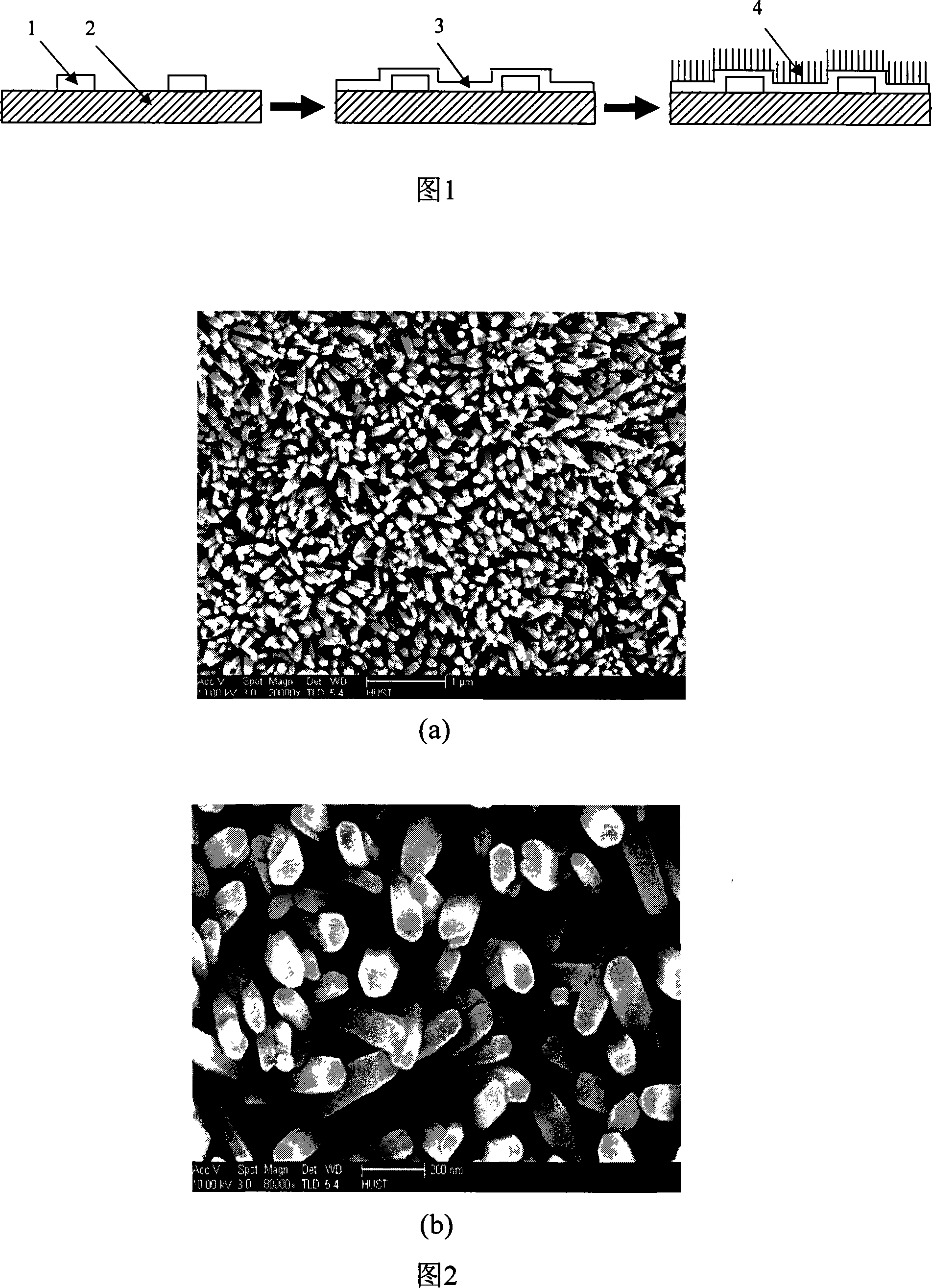
[0032] Pretreatment: Place the flat silicon substrate with heating and measuring electrodes in the alcohol solution of 0.5 mol / L zinc acetate and soak for 10 minutes, take it out and dry it at 80°C, and heat it at 350°C for decomposition. Repeat the above operation steps 5 times to form a layer of nano ZnO seed crystals on the substrate;

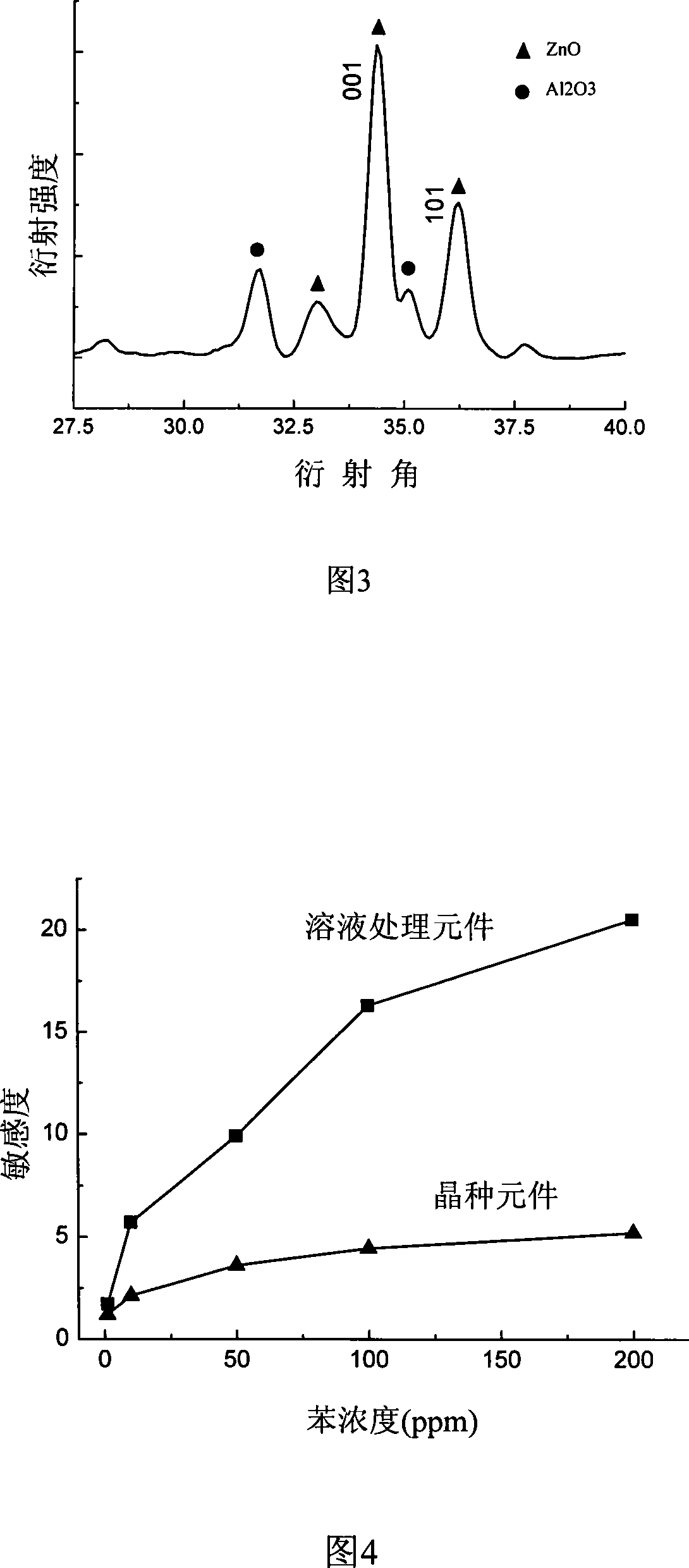
[0033] Solution treatment: add 0.6584 g of zinc acetate to 120 ml of deionized water, oscillate ultrasonically to form a uniform solution, drop into 320 μl of ethylenediamine, and transfer it to a sealable container. Suspend the flat substrate deposited with the ZnO seed crystal film in the solution, seal it with a cover, and place it in a water bath box at 80° C. for one and a half hours to keep warm. Take it out and cool it down to room temperature, wash it with deionized water for 15 minutes, put it in a drying oven for drying at 40°C, and then transfer it to a horse boiling furnace for sintering at 350°C to form a flat gas sensor (see Fi...

example 2

[0047] Pretreatment: Place the flat ceramic substrate with heating and measuring electrodes in the alcohol solution of 0.5 mol / L stannous sulfate and soak for 10 minutes, take it out and dry it at 80°C, and heat it to decompose at 400°C.

[0048] Repeat the above operation steps 5 times to form a layer of nano SnO on the substrate 2 Seed;

[0049] Solution treatment: Add 0.3187 g of stannous sulfate to 120 ml of dehydrated ethanol, oscillate with ultrasonic waves to form a uniform solution, drop into 320 μl of ethylenediamine, and transfer it into a sealable container. will deposit the SnO 2 The flat substrate of the seed crystal film is suspended in the solution, sealed with a cover, and kept in a water bath at 95°C for 24 hours. Take it out and cool it down to room temperature, wash it with deionized water for 15 minutes, put it in a drying oven for drying at 40°C, and then transfer it to a horse boiling furnace for sintering at 350°C to form a flat-plate gas sensor.

[0...

example 3

[0056] Pretreatment: Place the flat ceramic substrate with heating and measuring electrodes in the alcohol solution of 0.5 mol / L ferric nitrate and soak for 10 minutes, take it out and dry it at 80°C, and heat it to decompose at 350°C. Repeat the above steps 5 times to form a layer of nano-Fe on the substrate 2 o 3 Seed;

[0057] Solution treatment: Add 1.105g of ferric nitrate into 60ml of deionized water, and ultrasonically oscillate to form a uniform solution; at the same time, add 0.3g of sodium hydroxide to 60ml of deionized water and ultrasonically oscillate to form a uniform solution; in an airtight container. will deposit Fe 2 o 3 The flat substrate of the seed crystal film is suspended in the solution, covered and sealed, and kept in an 80° C. water bath for one and a half hours. Take it out and cool it down to room temperature, wash it with deionized water for 15 minutes, put it in a drying oven for drying at 40°C, and then transfer it to a horse boiling furnace...


PUM

PropertyMeasurementUnit
Lengthaaaaaaaaaa
Diameteraaaaaaaaaa

Abstract

The invention discloses a semiconductor oxide gas sensor component preparation method. (1)The invention cleans and dries a substrate printed with heating electrode and a measuring electrode, lays the substrate into water or alcohol solution with the soluble metal salts soaking, then dries, heats and decomposes the substrate, finally forms the seed crystal; (2) matches the water or the alcoholic solution with the homogeneous metallic ion soluble salt, adopts the same solvent dispensing precipitant solution, drips the solvent into the water or the alcoholic solution and mixes the solution evenly, then hangs and soaks the substrate in the solution, seals and heats up;(3) removes, washes, and sinters the substrate to obtain the gas sensor component. The traditional technique preparation of materials and components produced are separated. The invention utilizes simple technique preparing the high-sensitivity nanometer semiconductor oxide gas sensor component to overcome the shortcomings, and realizes the effective regulation to the surface sensitive components microstructure. The preparation method has the advantages that low requirements to the production equipment and environment, energy conservation, low cost, and mass production, therefore the invention is expected to be widely applied in the field of gas sensor.

Description

technical field [0001] The invention belongs to semiconductor materials, components and preparation technologies thereof, and relates to a method for preparing a material / component (sensor) integrated solution, in particular to a method for preparing a semiconductor oxide gas sensor. Background technique [0002] Gas sensors have been widely used in food hygiene, environmental monitoring, public safety, aerospace and other fields. Among various gas sensors, metal oxide sensors (gas sensors) have attracted attention due to their simple structure and low price. Sensitive material is the most important factor controlling the performance of gas-sensing elements, and sensitivity is the most basic and important performance index of gas-sensing materials, which is closely related to the microstructure of gas-sensing materials. Microscopic factors that affect sensitivity can be divided into two categories: (1) Geometric structure parameters: grain size and porosity, secondary parti...

Claims


Application Information

Patent Timeline
IPC IPC(8): G01N27/12H01L49/00
Inventor 曾大文谢长生胡木林蔡水洲夏先平张顺平
Owner HUAZHONG UNIV OF SCI & TECH
Learn More