Sub-wavelength micro-nano structure using polystyrol ball to focused photoetching form

A polystyrene ball, micro-nano structure technology, applied in the direction of micro-structure technology, micro-structure device, manufacturing micro-structure device, etc., can solve the problem of large target structure period and feature size, difficulty in forming nano-structure, and limitation of pattern size, etc. problems, to achieve the effect of reducing cycle and feature size, low cost, and easy operation

Inactive Publication Date: 2008-04-09
INST OF OPTICS & ELECTRONICS - CHINESE ACAD OF SCI
View PDF0 Cites 12 Cited by
  • Summary
  • Abstract
  • Description
  • Claims
  • Application Information

AI Technical Summary

Problems solved by technology

In recent years, the focus lithography method has gradually developed into a lithography method for making microstructures. It uses a microlens array or a structure equivalent to a microlens array to expose the resist, and uses the focusing effect of the lens to Form the maximum value of energy at the focal spot, and use the extremely high value of energy at the focal point to perform photolithography, thereby forming a nanostructure on the underlying photoresist. However, in the production process of this method, the traditional microlens array Generally, the caliber and numerical aperture are relatively large, so the period and feature size of the formed target structure are large. At the same time, because the size of the focal spot is limited by the diffraction limit, the size of the pattern is limited, which brings great challenges to the formation of nanostructures. difficulty

Method used


Image

  • Sub-wavelength micro-nano structure using polystyrol ball to focused photoetching form
  • Sub-wavelength micro-nano structure using polystyrol ball to focused photoetching form

Examples


Embodiment Construction

[0034] The present invention will be described in detail below in conjunction with the accompanying drawings and specific embodiments, but the scope of protection of the present invention is not limited to the following examples, but should include all content in the claims.

[0035] The concrete process of the embodiment of the present invention is as follows:

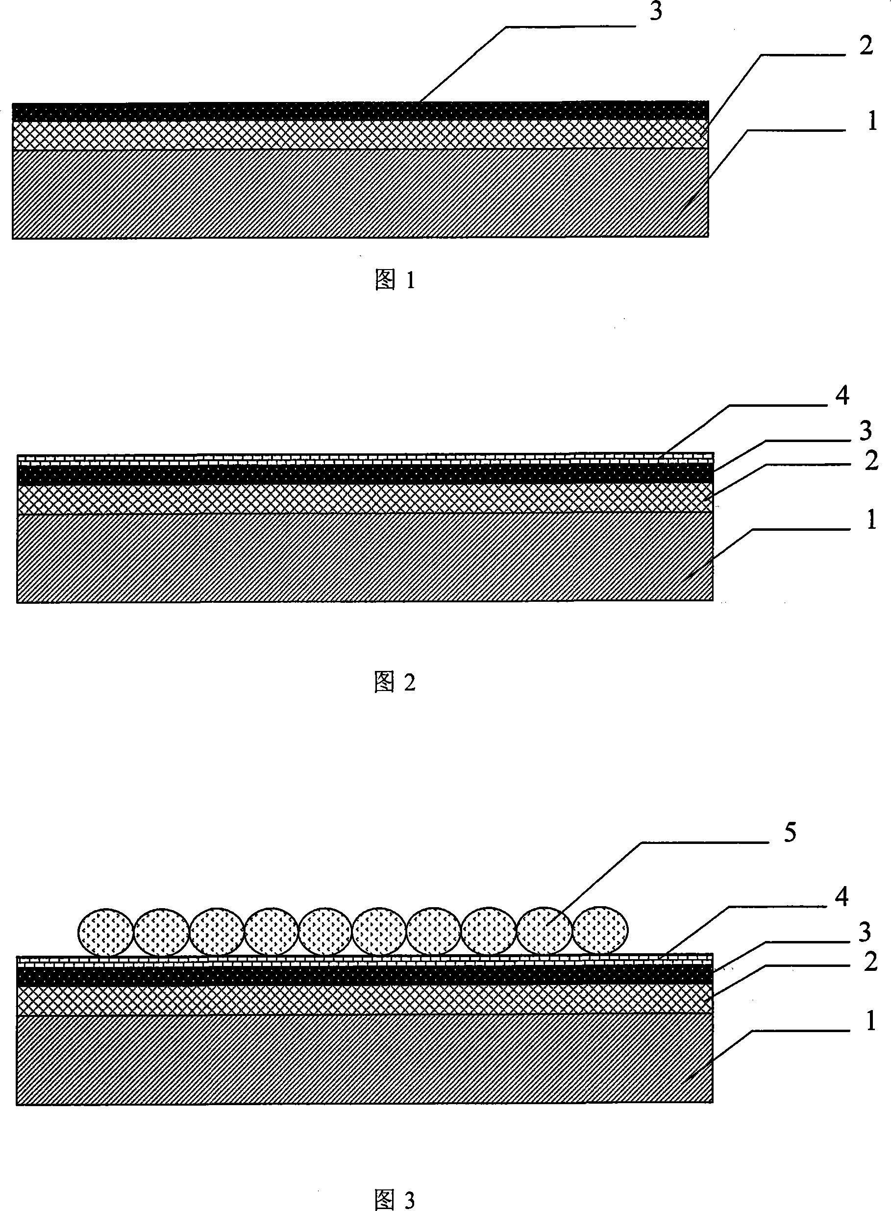
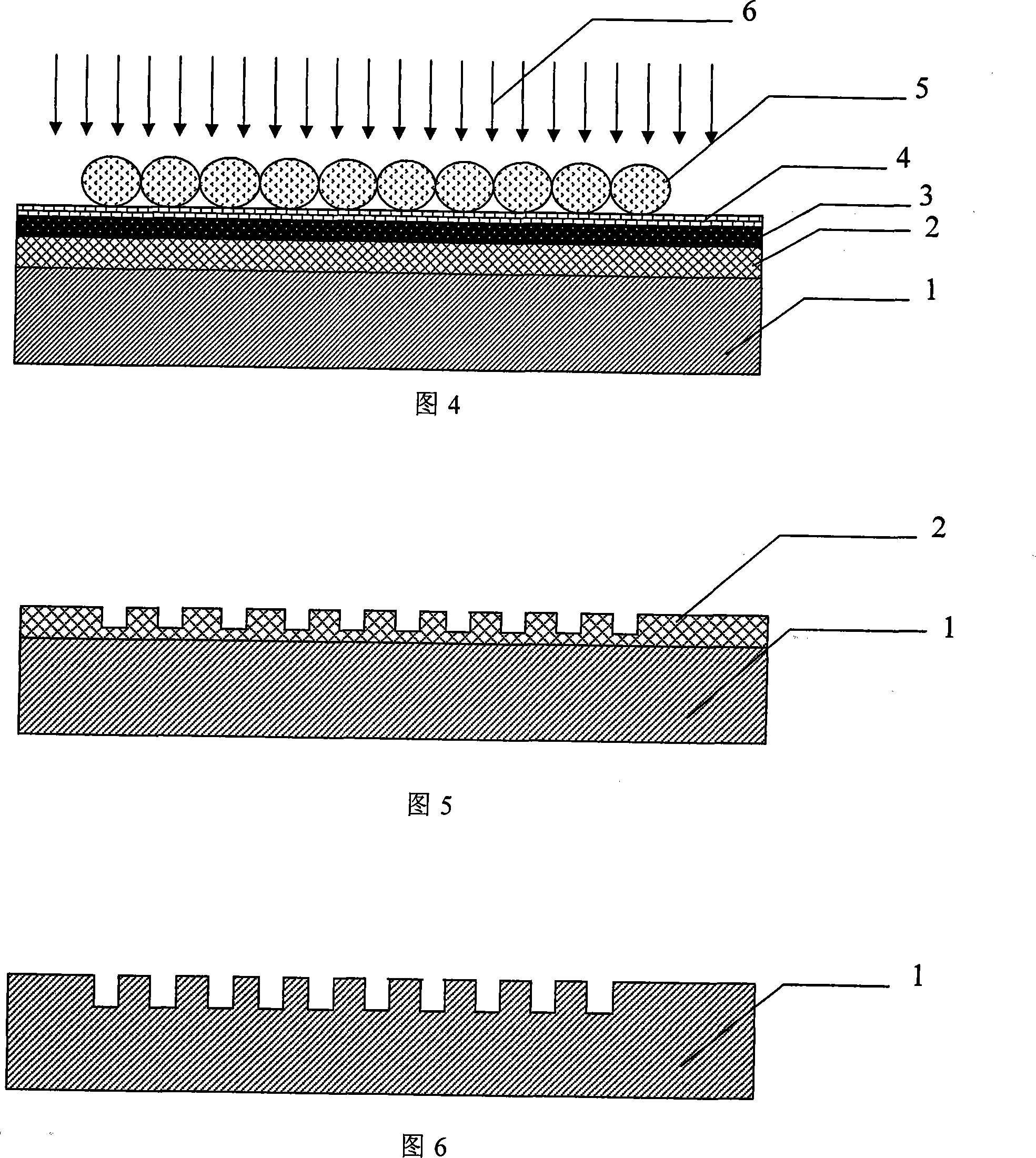
[0036] (1) Select silica S according to needs i o 2 The substrate was cleaned with acetone and ethanol, dried with high-pressure nitrogen, a layer of 200nm resist AZ3100 was spin-coated on the substrate surface, and a 40nm silver layer structure was deposited on the resist surface, as shown in the figure 1 shown;

[0037] (2) A polystyrene ball with a diameter of 3um is selected, and its focal length is calculated to be 2um.

[0038] (3) Spin-coat a layer of PMMA gap layer on the surface of the silver layer, its thickness is 1.8um, and its thickness is selected to make the focus of the incident light fall on the re...


PUM

PropertyMeasurementUnit
thicknessaaaaaaaaaa
thicknessaaaaaaaaaa
thicknessaaaaaaaaaa

Abstract

The present invention provides a production method used for focusing lithography forming sub-wavelength micro-nanostructure of polystyrene sphere, and is characterized in that: surface of substrate material firstly selected is sequentially in a spinning manner coated with a layer of anti-corrosion agent, evaporated with a layer of metal structure, then in a spinning manner coated with a layer of interval layer, and finally assembled with a layer of the polystyrene sphere. The structure is exposed in exposure system, then the polystyrene sphere, the interval layer and the metal layer structure are removed, the substrate is positioned into developing agent for development and obtainment of target structure, and finally the structure is transmitted to the substrate by etch of the target structure. The present invention adopts the polystyrene sphere as a focusing lens, further reduces the cycle and dimension of the lens, has stimulation of surface plasma inside the metal in the focusing and exposure as the metal structure is evaporated on the surface of the exposed anti-corrosion agent, improves resolution of a focusing focal spot, reduces the characteristic size of the forming targeted structure, and provides an effective method for the production of the sub-wavelength micro-nanostructure.

Description

technical field [0001] The invention relates to a method for making a nanostructure, in particular to a method for forming a sub-wavelength micro-nano structure by focusing photolithography using polystyrene balls. Background technique [0002] In recent years, with the rapid development of micro-nano processing technology and nanomaterials, the electromagnetic properties of micro-nano metal structures are receiving more and more attention. The interaction of light with surface micro-nano metal structures produces a series of new and exotic physical phenomena. For example, in 1998, French scientist Ebbesen and his collaborators discovered the phenomenon of extraordinary enhancement (Extraordinary Optical Transmission) of light passing through a subwavelength metal hole array. The research of H.J.Lezec et al. further showed that: when the light passes through the sub-wavelength metal nanohole, its transmittance can not only be enhanced, but also the diffraction angle of the ...

Claims


Application Information

Patent Timeline
Patent Type & Authority Applications(China)
IPC IPC(8): G03F7/00B81C1/00
Inventor 杜春雷李淑红董小春史立芳
Owner INST OF OPTICS & ELECTRONICS - CHINESE ACAD OF SCI
Why Eureka
Try Eureka