
Method for producing copper-indium-selenium thin-film solar cell wealthy-indium optical absorption layer

A solar cell and light-absorbing layer technology, which is applied in the manufacture of circuits, electrical components, and final products, to achieve the effects of compact structure, increased contact area, and safe and practical operation

Inactive Publication Date: 2008-04-09
UNIV OF SCI & TECH BEIJING
View PDF0 Cites 13 Cited by
  • Summary
  • Abstract
  • Description
  • Claims
  • Application Information

AI Technical Summary

Problems solved by technology

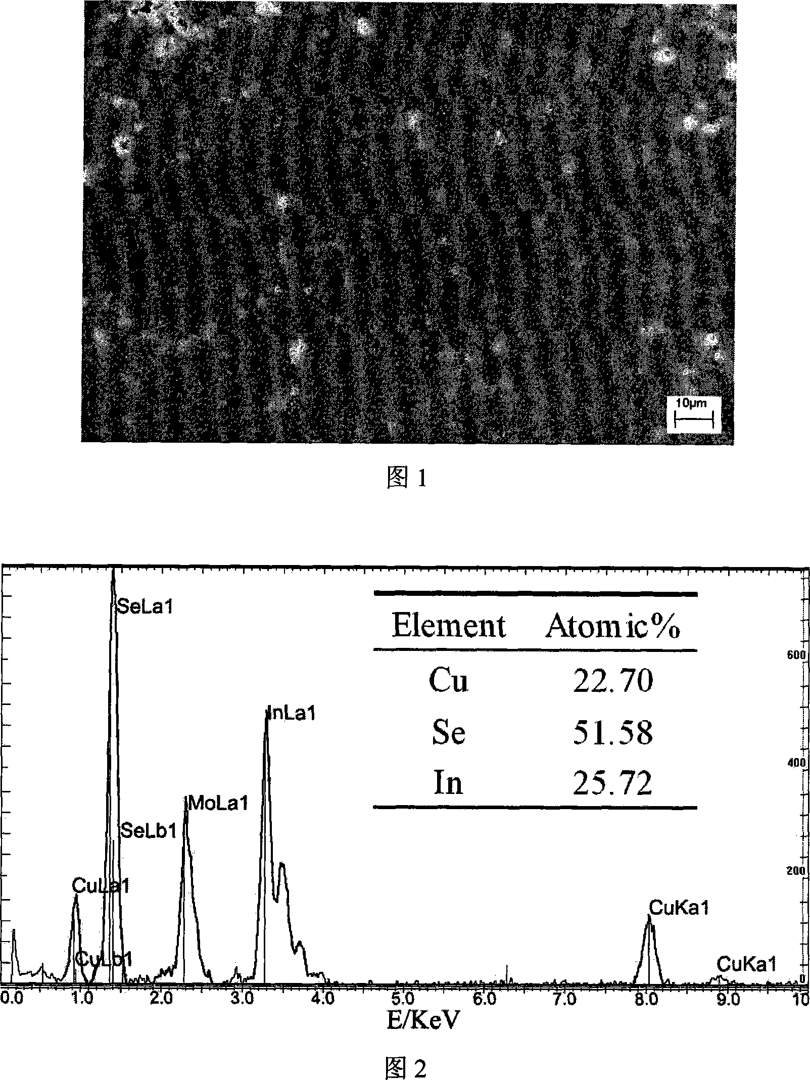
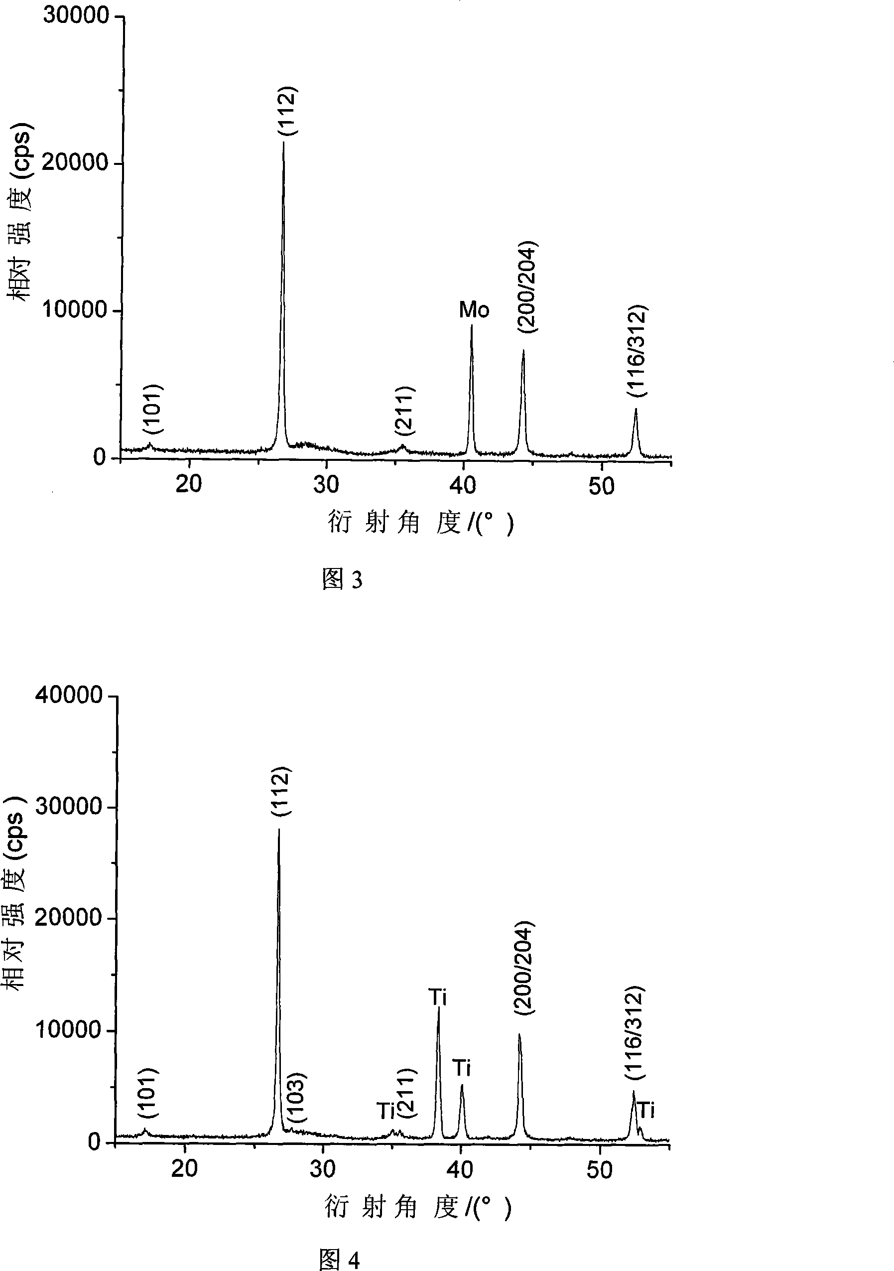
[0005] The object of the present invention is to provide a kind of CuInSe 2 A method for preparing an In-rich light-absorbing layer of a semiconductor thin-film solar cell, using a coating-sintering process to solve the problem of CuInSe 2 The improvement of In content in the semiconductor film and the problem of precise control make the obtained CuInSe 2 The thin film has the characteristics of In content slightly higher than Cu content, pure phase and compact microstructure, in order to meet the requirements for the preparation of high-efficiency CuInSe 2 Requirements for Thin Film Solar Cells

Method used


Image

  • Method for producing copper-indium-selenium thin-film solar cell wealthy-indium optical absorption layer
  • Method for producing copper-indium-selenium thin-film solar cell wealthy-indium optical absorption layer

Examples


Embodiment 1

[0016] Example 1: In-rich CuInSe 2 absorbing layer in H 2 Low temperature (400°C) preparation in atmosphere

[0017] (1) Apply a pressure of 200 MPa to the precursor film formed on the metal molybdenum substrate to make it dense, and then remove the pressure to obtain a dense precursor film.

[0018] (2) Place the above-mentioned precursor thin film in a resistance furnace, pass through H 2 Exclude the air, check the purity three times, raise the furnace temperature to 50°C, and preheat at 50°C for 10 minutes.

[0019] (3) Raise the temperature from 50°C to 230°C at a rate of 5°C / min, and keep the temperature for 1 hour.

[0020] (4) Heat up from 230°C to 400°C at a rate of 5°C / min, keep warm for 1 hour, then cool to room temperature with the furnace and take it out, and finally obtain a blue-black In-rich solar cell CuInSe 2 absorbent layer.

Embodiment 2

[0021] Example 2: In-rich CuInSe 2 absorbing layer in N 2 Low temperature (400°C) preparation in atmosphere

[0022] Operation process is the same as embodiment 1, will pass into H 2 The steps are replaced by passing into N 2 . Pass N 2 After 15 minutes of excluding the air, the resistance furnace was started to heat up. After the heat treatment, the blue-black In-rich solar cell CuInSe is finally obtained. 2 absorbent layer.

Embodiment 3

[0023] Example 3: In-rich CuInSe 2 absorbing layer in H 2 High temperature (550°C) preparation in the atmosphere

[0024] (1) Apply a pressure of 10 MPa to the precursor film formed on the metal molybdenum substrate to make it dense, and then remove the pressure to obtain a denser precursor film.

[0025] (2) Place the above-mentioned precursor thin film in a resistance furnace, pass through H 2 Exclude the air, check the purity three times, raise the furnace temperature to 50°C, and preheat at 50°C for 10 minutes.

[0026] (3) Raise the temperature from 50°C to 550°C at a rate of 10°C / min, keep it warm for 0.5 hours, and then cool it to room temperature with the furnace to take it out, and finally obtain a blue-black In-rich solar cell CuInSe 2 absorbent layer.


PUM


Abstract

The invention provides a method of preparing an In-enriched light absorption layer for a CuInSe2 thin-film solar battery, belonging to the preparation of CuInSe2 semiconductor thin films. The method adopts coating-sintering process, and uses Cu-In alloy, Cu-In alloy and Se powder as raw material. The method comprises mixing Cu-In alloy, Cu-In alloy and Se powder with a molar ratio of 1:(1.1-1.25):2:(2-2.2), ball milling the mixture for 36-72 hr to form a black precursor slurry; coating the slurry on a molybdenum foil substrate or a titanium foil substrate to form a precursor thin-film, and drying at low temperature; densifying the precursor thin-film by exerting 10-300 MPa pressure, and subjecting the precursor thin-film to heat treatment under H2 atmosphere, N2 atmosphere or vacuum. The method can accurately control the chemical composition in the precursor thin-film, can ensure the preparation of the In-enriched CuInSe2 semiconductor thin-film solar battery, and is more suitable for forming the absorption layer with uniform composition, compact structure, and flat surface. And, the sintering process is performed under innoxious atmosphere, so as to be safe and practice in operation.

Description

technical field [0001] The invention belongs to the technical field of new energy sources of photovoltaic materials, and relates to semiconductor CuInSe 2 Preparation of thin films, especially involving In-rich CuInSe 2 Preparation process of light absorbing layer of semiconductor thin film solar cell. Background technique [0002] CuInSe 2 It is a direct bandgap semiconductor compound with a chalcopyrite structure, which has a suitable bandgap (1.04eV), stable performance at room temperature, and no performance degradation effect (S-W effect) caused by light radiation. CuInSe 2 The photovoltaic conversion efficiency of thin-film solar cells has exceeded 20%, making CuInSe 2 It has become a promising photovoltaic material. [0003] Due to CuInSe 2 The unique intrinsic defect self-doping ability of the material makes it have strong composition tolerance, and CuInSe, which is poor in Cu and rich in In 2 Thin film (CuInSe with In content greater than Cu content 2 thin f...

Claims


Application Information

Patent Timeline
Patent Type & Authority Applications(China)
IPC IPC(8): H01L31/18
CPCY02P70/50
Inventor 果世驹聂洪波王延来王义民杨霞
Owner UNIV OF SCI & TECH BEIJING
Learn More