P type GaN cadmium-indium-oxygen transparent electrode and method for producing the same

A technology of transparent electrodes and transparent conductive films, applied in circuits, electrical components, laser parts, etc., can solve problems such as affecting the uniform current diffusion and thermal stability, reducing specific contact resistivity, and reducing the concentration of P-type GaN holes. , to achieve high industrial utilization value and improve the effect of responsiveness

Inactive Publication Date: 2008-04-16
CHONGQING UNIV
View PDF0 Cites 8 Cited by
  • Summary
  • Abstract
  • Description
  • Claims
  • Application Information

AI Technical Summary

Problems solved by technology

[0003] The main problems of using Ni / Au metal as P-type GaN contact electrodes on GaN-based LEDs are: when Ni / Au is too thin, it will affect the uniform diffusion of current and thermal stability; when it is too thick, the light transmittance of the metal film is low, Greatly reduces LED luminous efficiency
[0010] But directly put CdIn 2 o 4 The film is deposited on P-type GaN, and it is difficult to obtain ohmic contact after alloying treatment. The reasons are: (1) P-type GaN has a band gap of 3.4eV, an electron affinity of 4.1eV, and a large work function (7.5eV). with CdIn 2 o 4 The barrier height formed by the contact is large; (2) P-type GaN is difficult to achieve heavy doping, usually the doping concentration of Mg in P-type GaN is 10 20 cm -3 , but because Mg will form a deep main energy level in P-type GaN, and its ionization energy is very high (~170meV), according to Fermi-Dirac statistics, the ionization rate of Mg dopant is about 1%, As a result, the carrier concentration is difficult to exceed 10 18 cm -3 ; In addition, Mg can also form a complex Mg-H with hydrogen in the material (that is, hydrogen passivation), and compensate some residual acceptor impurities, so that the hole concentration of P-type GaN is further reduced, which limits the formation of low-resistance Tunneling current required for ohmic contact; (3) During the process, it is easy to generate N vacancies as donors on the surface of P-type GaN, reducing the hole concentration on the surface of P-type GaN
In addition, the conditions of the metallization process will also affect the P-type GaN contact resistivity
Therefore, to form an ohmic contact on P-type GaN, it is necessary to reduce the barrier height, so consider inserting an intermediate metal layer between the transparent oxide film and the semiconductor substrate to reduce the barrier height, thereby reducing the specific contact resistivity

Method used


Image

  • P type GaN cadmium-indium-oxygen transparent electrode and method for producing the same
  • P type GaN cadmium-indium-oxygen transparent electrode and method for producing the same

Examples


Embodiment 1

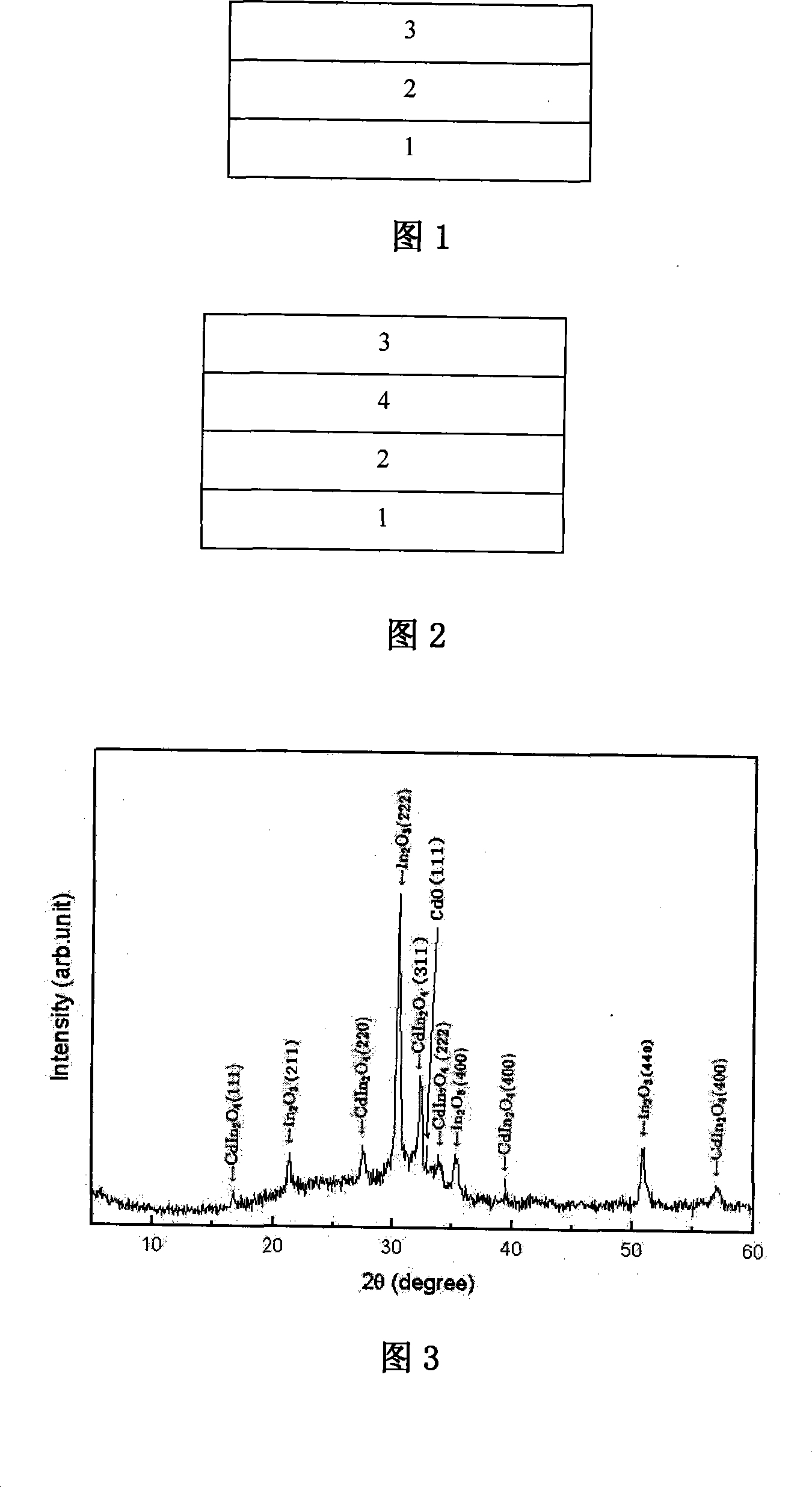
[0033] Embodiment 1: referring to accompanying drawing 1, a P-type GaN 1 has a first conductive layer 2 on the P-type GaN 1, and is characterized in that: a CIO transparent conductive film 3 is arranged on the first conductive layer 2, and this example is When the conductive layer only comprises the first conductive layer 2, the steps are as follows:

[0034] 1) P-type GaN 1 (carrier concentration 3.37×10 17 cm -3 , mobility 4.34cm 2 / V.s) Immerse in aqua regia solution for 3-5 minutes, and use acetone, alcohol and deionized water to vibrate ultrasonically for 5 minutes respectively (the purpose is to remove surface impurities and oxide layers to reduce the barrier height);

[0035]2) Blow dry the sample obtained in the previous step with nitrogen, immediately place it in an electron gun evaporation system, vacuumize it, and evaporate and deposit a metal Ni (ie, the first conductive layer 2) with a thickness of 5 nm on the P-type GaN 1. The process conditions are: high volt...

Embodiment 2

[0042] Embodiment 2: referring to accompanying drawing 1, accompanying drawing 2, this example is the situation of re-depositing a second conducting layer 4 between the first conducting layer 2 and the CIO transparent conducting film 3, and its steps are as follows:

[0043] 1) Immerse P-type GaN 1 in aqua regia solution for 3-5 minutes, and use acetone, alcohol and deionized water to ultrasonically oscillate for 5 minutes respectively (the purpose is to remove surface impurities and oxide layers to reduce the barrier height);

[0044] 2) Dry the sample obtained in the previous step with nitrogen, immediately place it in the electron gun evaporation system, vacuumize it, and evaporate and deposit metal Ni (ie, the first conductive layer 2) with a thickness of 5 nm on the P-type GaN 1, and then use The same method deposits a layer of 5nm thick gold Au (i.e. the second conductive layer 4), and its process conditions are: high voltage 6KV, beam current 155mA, working pressure: 2.2...


PUM

PropertyMeasurementUnit
thicknessaaaaaaaaaa
thicknessaaaaaaaaaa
diameteraaaaaaaaaa

Abstract

The present invention discloses a cadmium indium oxygen (CIO) transparent electrode of P-type GaN; with the adoption of the CIO transparent conductive film structure, the light transmittance of the transparent electrode improves more 15 percent than that of the prior metal (Ni or Ni/Au) electrode; the invention can be applied to GaN-based blue-ray light-emitting diodes or laser diodes to improve luminous efficiency or can be applied to GaN-based photodetectors to improve responsivity, thereby having high industrial utility value. The invention also discloses a preparation method of transparent electrode which solves the problem that the COI transparent conductive film is difficult to achieve ohmic contact on the P-type GaN.

Description

technical field [0001] The invention relates to an ohmic contact scheme on P-type GaN and a preparation method thereof, in particular to a cadmium indium oxide transparent electrode on P-type GaN and a preparation method thereof. Background technique [0002] GaN-based materials are representative of the third-generation wide-bandgap semiconductor materials. They have many excellent properties and have broad application prospects in many fields of optoelectronic and microwave devices such as blue and violet light emission, ultra-high frequency, high temperature, and high power. With the commercialization and practical application of high-brightness baskets and purple GaN-based LEDs, high-brightness white LEDs may replace various current lighting lamps, and lighting technology is facing a new revolution. However, there are still some technical problems that have not been completely resolved in the production of GaN-based LEDs. One of the most important problems is that it is ...

Claims


Application Information

Patent Timeline
Patent Type & Authority Applications(China)
IPC IPC(8): H01L33/00H01S5/00H01L33/42
Inventor 方亮张淑芳彭丽萍董建新刘高斌
Owner CHONGQING UNIV
Why Eureka
Try Eureka