Curved substrate multi-phase micro-optical element processing method based on flexible ultraviolet die mold

A micro-optical and multi-phase technology, which is applied in the photoplate making process of optical elements, pattern surface, optics, etc., can solve the problems of inability to realize processing and limited application, and achieve easy batch and rapid processing, simple processing technology, The effect of low processing cost

Inactive Publication Date: 2008-07-16
HARBIN INST OF TECH
View PDF0 Cites 24 Cited by
  • Summary
  • Abstract
  • Description
  • Claims
  • Application Information

AI Technical Summary

Problems solved by technology

[0005] Currently, there are published methods for fabricating microstructured optical elements on curved substrates based on flexible stamper UV imprinting technology, such as ①Younan Xia, George M.Whitesides.Soft Lithography.Angew.Chem.Int.Ed.Vol 37:550~575( 1998) ②Xia YN, Kim E, Zhao XM, Rogers JA, Prentiss M, Whitesides GM.Complex optical surfaces formed by replica molding against elastomeric masters.SCIENCE 273(5273):347~349(1996), etc., by using flexible stamping mold PDMS realizes microstructure processi

Method used


Image

  • Curved substrate multi-phase micro-optical element processing method based on flexible ultraviolet die mold
  • Curved substrate multi-phase micro-optical element processing method based on flexible ultraviolet die mold
  • Curved substrate multi-phase micro-optical element processing method based on flexible ultraviolet die mold

Examples


Embodiment 1

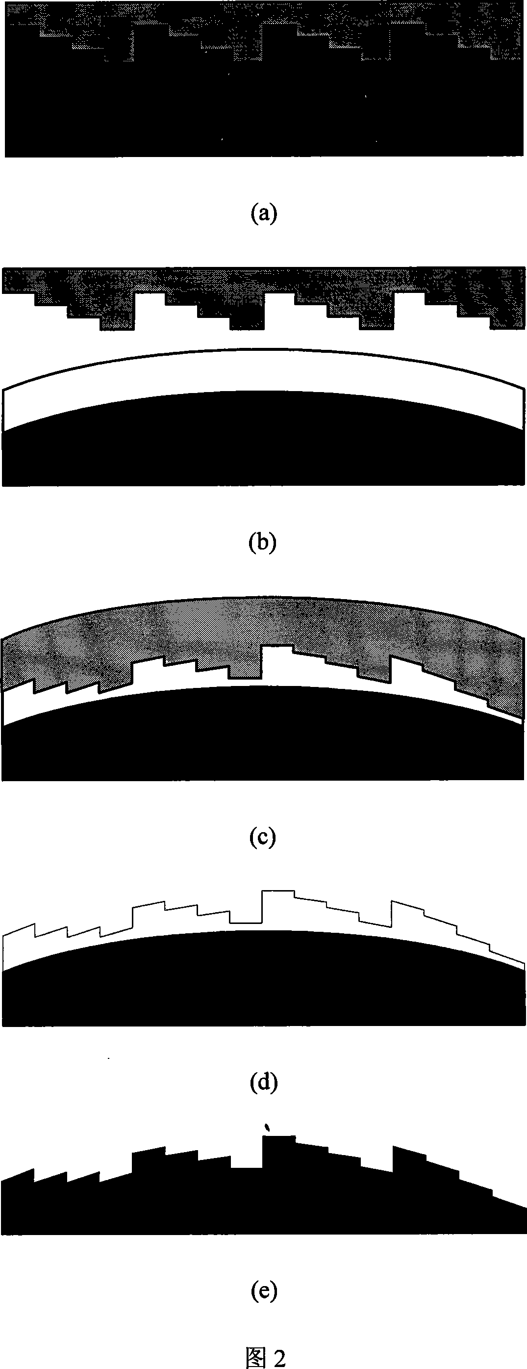
[0044] As shown in Figure 2, the diffractive optical lens with spherical base multi-step micro-relief structure is made, the element material is glass, the stamper material is PDMS, and the polymer required for UV imprinting is UV-curable glue OG154. The specific process is as follows:

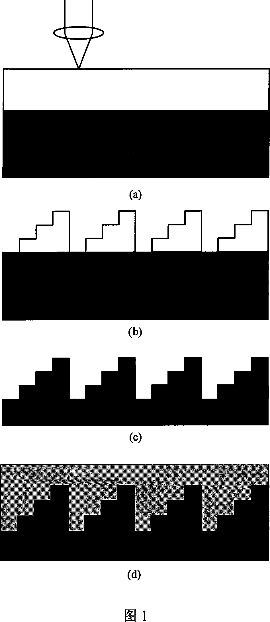
[0045] 1. As shown in Figure 1, laser direct writing technology is used to produce a surface relief quartz master with the same structure as the target.

[0046] 2. As shown in Figure 2(a), the microstructure injection molding replication technology is used to replicate the microstructure of the master plate to the surface of the PDMS material.

[0047]3. As shown in Figures 2(b) and 2(c), the PDMS stamper is used to carry out UV imprinting on the spherical substrate, and the PDMS stamper is bent into a curved surface similar to the processed spherical surface under the action of external force.

[0048] 4. As shown in Fig. 2(d), it is the spherical polymer micro-relief structure after demould...

Embodiment 2

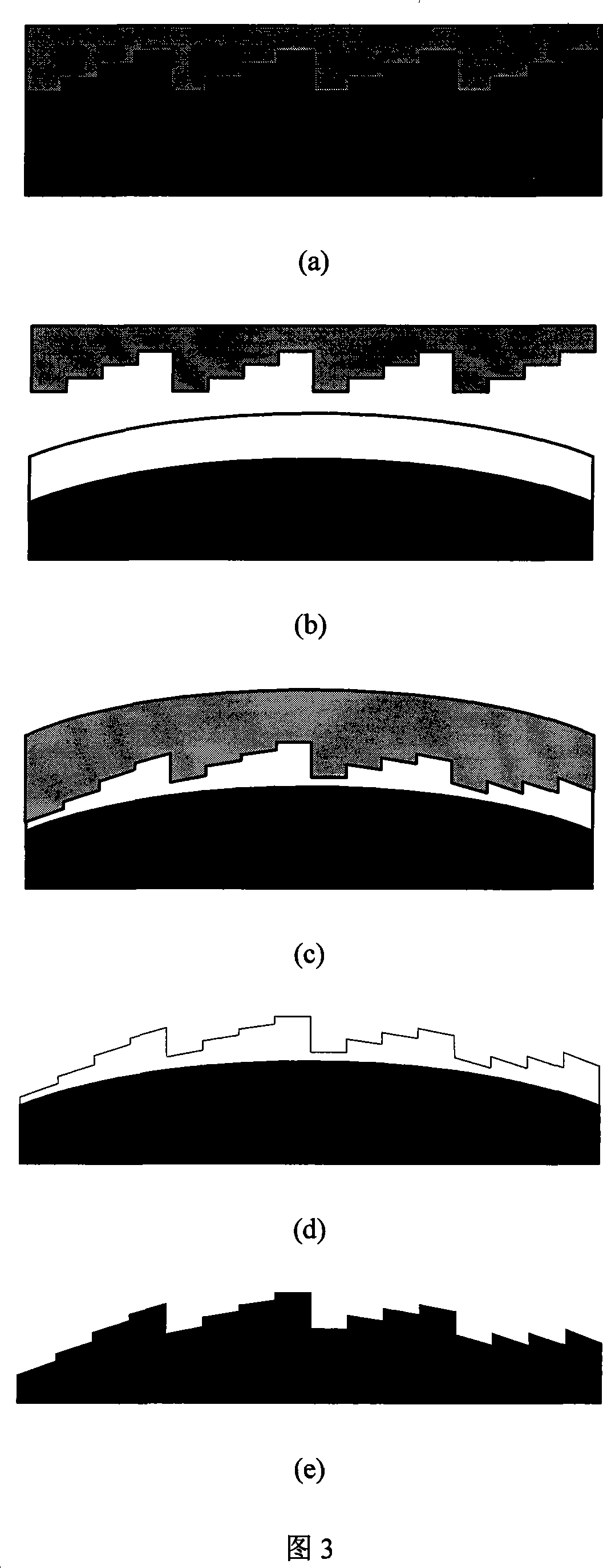
[0051] As shown in Figure 3, a binary optical element with a multi-step structure on a cylindrical base is fabricated. The material of the element is single crystal silicon, the material of the mold is PDMS, and the polymer is an ultraviolet organic photosensitive solvent PAK01. The specific process is as follows:

[0052] 1. As shown in Figure 1, apply electron beam direct writing technology to make a quartz mother board with the same structure as the target.

[0053] 2. As shown in Figure 3(a), the microstructure of the master plate is copied to the surface of the PDMS material by using the microstructure injection molding replication technology.

[0054] 3. As shown in Figure 3(b) and 3(c), apply the PDMS stamper to implement UV imprinting on the cylindrical substrate, and the PDMS stamper is bent into a curved surface similar to the processed cylindrical surface under the action of external force shape.

[0055] 4. As shown in Fig. 3(d), it is the columnar-based polymer ...

Embodiment 3

[0058] As shown in Figure 4, the Fresnel lens with a continuous relief structure is produced, the element material is sapphire, the molding material is PDMS, and the polymer is selected from the ultraviolet organic photosensitive solvent PAK01. The specific process is as follows:

[0059] 1. As shown in Figure 1, apply the electron beam direct writing technology to make a continuous relief structure quartz mother board with the same structure as the target.

[0060] 2. As shown in Figure 4(a), the microstructure injection molding replication technology is used to replicate the microstructure of the master plate to the surface of the PDMS material.

[0061] 3. As shown in Figure 4(b) and 4(c), the PDMS stamper is used to implement UV imprinting on the aspheric substrate, and the PDMS stamper is bent into a curved shape similar to the processed aspheric surface under the action of external force appearance.

[0062] 4. As shown in Figure 4(d), it is the aspherical polymer micro...


PUM


Abstract

The invention relates to a method for processing curved-surface substrate multi-phrase micro optical elements and a technique of manufacturing the micro optical elements based on a flexible UV pressing die; the method has an additional step which takes a polymer structure as a mask and uses a dry etching technique to form an embossed structure on a substrate to complete the graph transmission form a fine structure to the surface of a hard substrate; a stamping step in which a flexible pressing die creates elastic deformation with external prestress applied during the stamping process to bend into a shape similar to a surface being processed, with the deflection worked out by a method of FEM ( finite element method) simulation; and a step for making a motherboard, in which the shape and size of a fine structure on the surface of a pressing die motherboard is designed according to the deflection for compensation. The method can be used to realize the processing and manufacture of micro optical elements which have a curved-surface substrate of single material and are made of non-polymer hard materials.

Description

technical field [0001] The invention belongs to a manufacturing method of a micro-optical element, and relates to a method for processing a multi-phase micro-optical element of a curved surface base based on a flexible ultraviolet pressure mold. Background technique [0002] Microstructured optical elements based on curved substrates have better optical imaging characteristics than diffractive optical elements based on planar substrates. The application of microstructured optics on curved substrates in optical systems can greatly improve the integration of optical systems and increase optical The design freedom of the system, the reduction of volume, the compression of cost, and the reduction of the difficulty of optical system design maximize the performance of the optical system. [0003] The traditional optical lithography method is difficult to apply to the microstructure processing of curved substrates. At present, the processing of microstructured optical elements on c...

Claims


Application Information

Patent Timeline
IPC IPC(8): G03F7/00G03F7/20G02B1/02
Inventor 金鹏刘楠朱鹏谭久彬
Owner HARBIN INST OF TECH
Why Eureka
Try Eureka