Preparation of silicon nanowire array

A technology of silicon nanowire arrays and silicon nanowires, which is applied in the field of nanomaterials, can solve the problems of increased cost, difficulty in obtaining silicon nanowires with uniform diameter and orderly arrangement, and reduced production efficiency of silicon nanowires, and achieves the effect of simple conditions

Inactive Publication Date: 2008-11-12
BEIJING NORMAL UNIVERSITY
View PDF1 Cites 26 Cited by
  • Summary
  • Abstract
  • Description
  • Claims
  • Application Information

AI Technical Summary

Problems solved by technology

Although this technique can be applied to silicon substrates with different doping types, concentrations and orientations, and can control the length and crystallographic orientation of nanowires, it is difficult to obtain silicon nanowires with uniform diameter and orderly arrangement.
Our research ...

Method used


Image

  • Preparation of silicon nanowire array

Examples


Embodiment 1

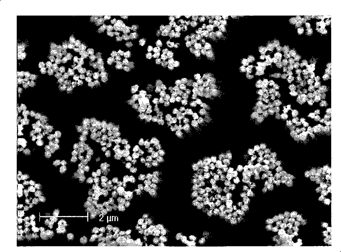
[0026] According to the surface area of ​​the silicon substrate, drop the silicon dioxide pellet solution with a concentration of 0.1% onto the surface of the cleaned silicon wafer, and let it dry naturally. The silicon substrate on which the silicon dioxide balls are arranged is annealed for 3 hours at a temperature of 900 degrees Celsius under the protection of argon and hydrogen. Then use diluted hydrofluoric acid to corrode the balls for 5 minutes, and then deposit a 30nm thick Ag film by electroplating on the surface of the silicon chip array of the ball array, and then immerse the sample deposited with the silver film in a solution containing hydrofluoric acid and hydrogen peroxide. Silicon nanowires and their arrays arranged in a large area can be obtained by treating hydrogen oxide mixed solution in a closed container kettle (concentrations of hydrofluoric acid and hydrogen peroxide are 1.0 mol / L and 0.1 mol / L respectively) for 10 minutes .

Embodiment 2

[0028] According to the surface area of ​​the silicon substrate, a solution of 0.3% silicon dioxide spheres was dropped onto the surface of the cleaned silicon wafer and allowed to dry naturally. The silicon substrate on which the silicon dioxide balls are arranged is annealed for 3 hours at a temperature of 950 degrees Celsius under the protection of argon and hydrogen. Then use diluted hydrofluoric acid to corrode the balls for 10 minutes, and then use vacuum thermal evaporation to deposit a 30nm thick Ag film on the surface of the silicon chip array with the ball array, and then immerse the sample with the silver film deposited in the hydrofluoric acid solution. and hydrogen peroxide mixed solution in a closed container kettle (concentrations of hydrofluoric acid and hydrogen peroxide are 4.0mol / L and 0.1mol / L respectively) for 30 minutes to obtain large-area ordered silicon nanowires and its array.

Embodiment 3

[0030]According to the surface area of ​​the silicon substrate, drop the silicon dioxide pellet solution with a concentration of 1.0% onto the surface of the cleaned silicon wafer, and let it dry naturally. The silicon substrate on which the silicon dioxide balls are arranged is annealed for 3 hours at a temperature of 950 degrees Celsius under the protection of argon and hydrogen. Then, the silicon substrate on which the silicon dioxide spheres are arranged is annealed for 3 hours at a temperature of 950 degrees Celsius under the protection of argon and hydrogen. Then use diluted hydrofluoric acid to corrode the balls for 15 minutes, and then deposit a 50nm thick Ag film by electroplating on the surface of the silicon wafer with the array of small balls, and then immerse the sample deposited with the silver film in a solution containing hydrofluoric acid and hydrogen peroxide. The silicon nanowires and their arrays arranged in a large area can be obtained by treating the hydr...


PUM


Abstract

The invention relates to a method for preparing silicon nanowires, belonging to the nanophase material preparation technical field. The method comprises the following steps that: a silicon chip is washed and shaken by acetone and alcohol and is processed by an acid cleaning liquid and a No.1 standard cleaning solution; a silicon dioxide spheres solution with a weight percentage density between 0.02 and 2.0 percent is added on the silicon chip surface which is washed off in the step one drop by drop by a micro pipette, the processed silicon chip is placed in air to air naturally; the silicon chip with silicon dioxide sphere arrays is annealed for one to three hours at a temperature of between 900 and 1000 DEG C; afterwards, the silicon chip is put into a diluent hydrofluoric acid solution to be eroded for 2 to 20 minutes so that the diameters of the spheres become small; an Ag film with a thickness between 20 and 80nm is deposited on the silicon chip surface by the plating technique or the vacuum evaporating technique; and a sample deposited with the Ag film is dipped into the hydrofluoric acid and hydrogen peroxide etching solution (or ferric nitrate) to be eroded for 4 to 100 minutes. The preparation method can rapidly prepare a large area of silicon nanowire arrays, thereby being suitable for the large-scale industrial production.

Description

technical field [0001] The invention relates to a method for preparing silicon nanowires, which belongs to the technical field of nanomaterials. Background technique [0002] One-dimensional semiconductor nanomaterials have broad application prospects in future mesoscopic and nano-optoelectronic devices due to their unique structures and physical properties. Due to the important position of silicon materials in the traditional microelectronics industry, the research of one-dimensional silicon nanowires has received great attention. The current nano-silicon wire preparation methods mainly include chemical vapor deposition and oxide-assisted growth techniques. Due to the limitations of the growth mechanism, these methods usually require relatively high temperatures and some complicated equipment, resulting in high production costs. For example, the silicon wire growth temperature in patent 00117242.5 is as high as 1600-2000°C [refer to: Chinese patent 00117242.5, publication...

Claims


Application Information

Patent Timeline
IPC IPC(8): C04B41/52B82B1/00B82B3/00
Inventor 彭奎庆李述汤
Owner BEIJING NORMAL UNIVERSITY
Why Eureka
Try Eureka