Metal semiconductor field effect light emitting transistor and preparing method thereof

A technology of light-emitting transistors and metal semiconductors, applied in semiconductor devices, electrical components, circuits, etc., can solve problems affecting device characteristics, etching products and mask material pollution, n-type GaN Schottky contact effects, etc.

Inactive Publication Date: 2008-11-19
SOUTH CHINA NORMAL UNIVERSITY
View PDF0 Cites 5 Cited by
  • Summary
  • Abstract
  • Description
  • Claims
  • Application Information

AI Technical Summary

Problems solved by technology

However, the etching damage introduced by dry etching has a serious adverse effect on the optical and electrical characteristics of the device. For example, the bombardment of high-energy ions in etching causes a large number of point defects and defect clusters, etch products and mask materials. Contamination, surface roughening, and the introduction of other impurities, etc., will affect the characteristics of the device
ICP etching will introduce damage on the GaN surface, forming electron trap energy levels, which will cause the Schottky barrier height to decrease, the ideality factor to increase, and the reverse leakage current to increase, etc.
These damages are not a concern for n-type GaN ohmic contacts, because the reduction of n-GaN surface resistivity after etching is conducive to the formation of n-type ohmic contacts, but it has a great impact on n-type GaN Schottky contacts. influences
For example, the etching damage introduced during the trench gate fabrication process will cause the characteristics of GaN FET to degrade

Method used


Image

  • Metal semiconductor field effect light emitting transistor and preparing method thereof
  • Metal semiconductor field effect light emitting transistor and preparing method thereof
  • Metal semiconductor field effect light emitting transistor and preparing method thereof

Examples


Embodiment 1

[0023] Metal-semiconductor field-effect light-emitting transistors are prepared according to the following steps, and the substrate is GaN:

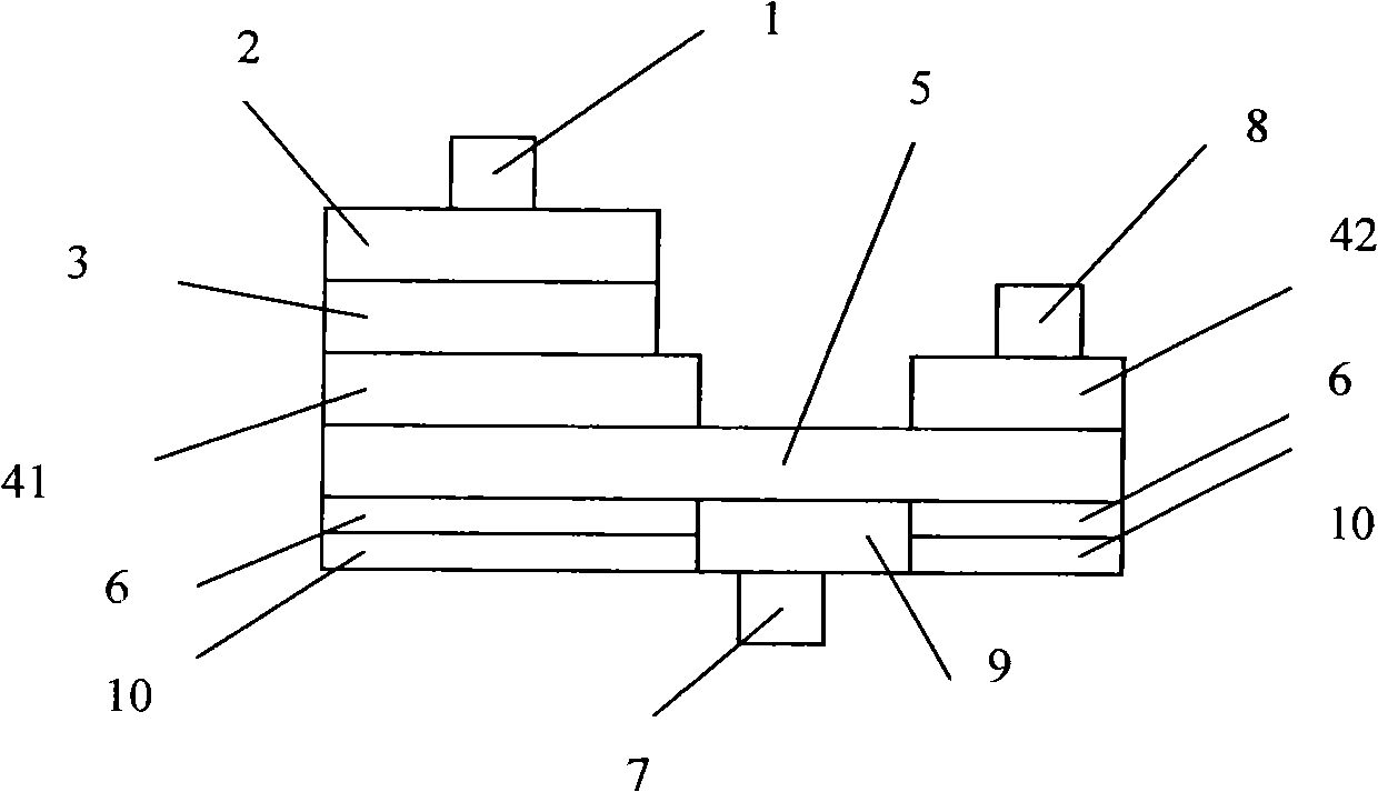
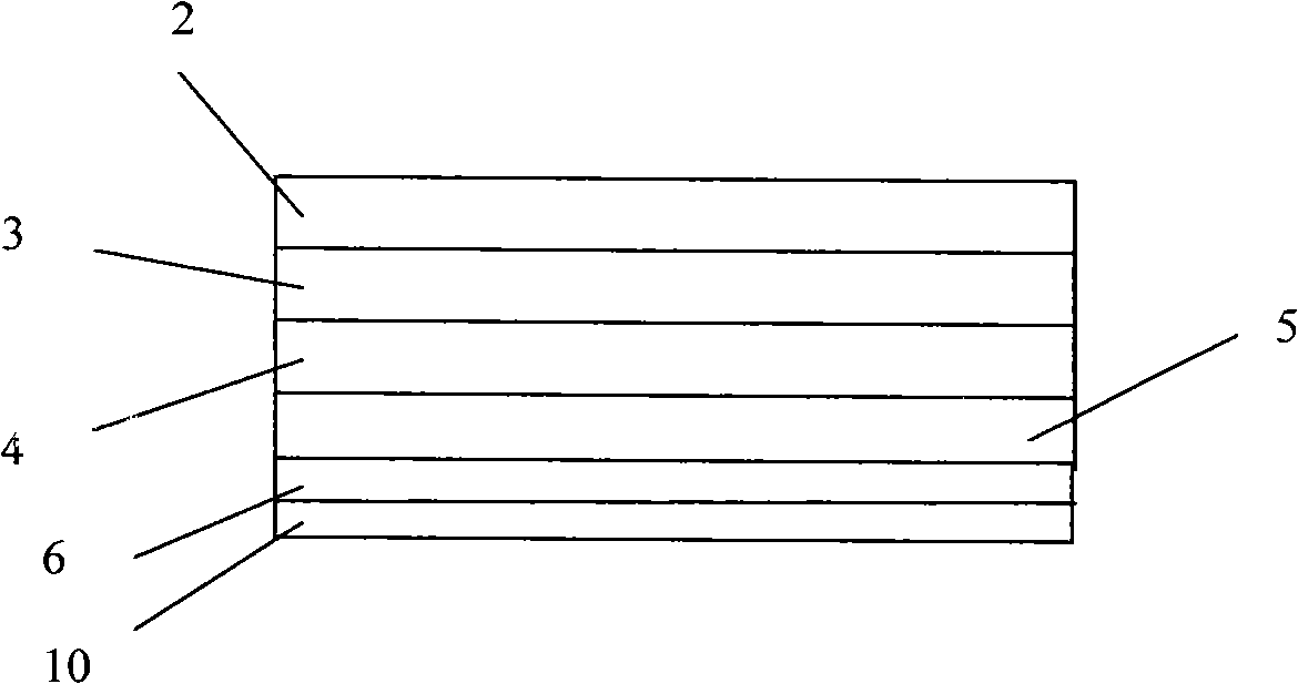
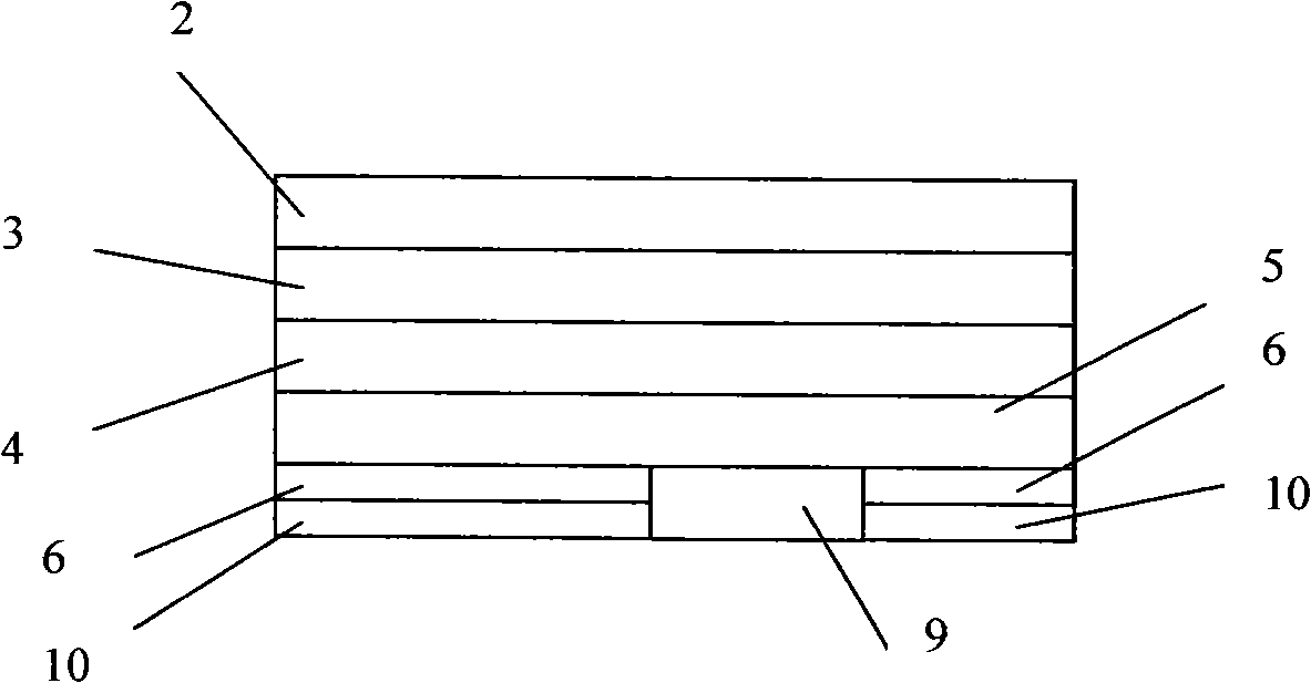
[0024] (1) if figure 2 As shown, a 2.0um thick GaN buffer layer 6 is grown on a square sapphire substrate 10;

[0025] (2) if figure 2 As shown, a 3.0um thick low-doped n-type layer 5 is grown on the buffer layer 6, GaN is doped with Si, and the doping concentration is 10 17 cm -3 ;

[0026] (3) if figure 2 As shown, continue to grow a 3um thick highly doped n-type layer 4 as the electron emission region, GaN doped with Si, and the doping concentration is 10 19 cm -3 ;The forbidden band width is 3.4eV;

[0027] (4) if figure 2 As shown, continue to grow the superlattice structure of GaN / InGaN material to form a multi-quantum well layer 3, which serves as the high-brightness active light-emitting region of the transistor, forming 10-20 quantum wells, and the thickness of the active region is 150-300nm;

[0028] (5) if figur...

Embodiment 2

[0035] Metal-semiconductor field-effect light-emitting transistors are prepared according to the following steps, and the substrate is GaN:

[0036] (1) if figure 2 As shown, a 2.0um thick GaN buffer layer 6 is grown on a square sapphire substrate 10;

[0037] (2) if figure 2 As shown, a 3.0um thick low-doped n-type layer 5 is grown on the buffer layer 6, GaN is doped with Si, and the doping concentration is 10 17 cm -3 ;

[0038] (3) if figure 2 As shown, continue to grow a 3um thick highly doped n-type layer 4 as the electron emission region, GaN doped with Si, and the doping concentration is 10 19 cm -3 ;The forbidden band width is 3.4eV;

[0039] (4) if figure 2 As shown, continue to grow the superlattice structure of GaN / InGaN material to form a multi-quantum well layer 3, which serves as the high-brightness active light-emitting region of the transistor, forming 10-20 quantum wells, and the thickness of the active region is 150-300nm;

[0040] (5) if figur...


PUM


Abstract

The invention discloses a metal semiconductor field effect transistor and the fabrication method thereof. The metal semiconductor field effect transistor comprises a substrate, a buffer layer which is arranged on the substrate, a first n type heavily doped layer above the buffer layer, a multi-quantum well layer and a p type layer which are sequentially arranged on the n type layer, a second n type heavily doped layer above the buffer layer, a source electrode which is in Ohmic contact with the second n type heavily doped layer, and a drain electrode which is in Ohmic contact with the p type layer. The first n type heavily doped layer is not connected with the second n type heavily doped layer. The metal semiconductor field effect transistor is characterized in that a slightly doped n type layer is arranged between the buffer layer and first and second n type heavily doped layers, and a SiO2 layer connected with the slightly doped n type layer is embedded between the substrate and the buffer layer. The metal semiconductor field effect transistor further comprises a gate electrode which is in Schottky contact with the SiO2 layer. The metal semiconductor field effect transistor reduces etching damages, thus improving the performance of the components.

Description

technical field [0001] The invention relates to a light-emitting transistor and belongs to the field of semiconductor devices. Background technique [0002] Wide bandgap semiconductor GaN is an ideal material for preparing optoelectronic devices (LED, LD, etc.) and high-temperature and high-power electronic devices (MESFET, HEMT, etc.). Due to the difficulty of growing GaN bulk crystals, most GaN materials are made by heteroepitaxy on sapphire or semi-insulating SiC substrates. Therefore, when manufacturing GaN devices, in order to lead out electrodes, n-type GaN For Schottky contacts, etching is essential. GaN has strong chemical stability, and there is no effective wet chemical etching solution at present. Therefore, dry etching is used in the device manufacturing process. At present, inductively coupled plasma (ICP) etching is widely used in GaN technology. eclipse. However, the etching damage introduced by dry etching has a serious adverse effect on the optical and el...

Claims


Application Information

Patent Timeline
Patent Type & Authority Applications(China)
IPC IPC(8): H01L33/00H01L33/02H01L33/36
Inventor 郭志友曾坤赵华雄高小奇孙慧卿范广涵
Owner SOUTH CHINA NORMAL UNIVERSITY
Why Eureka
Try Eureka