Method of preparing type p ZnO nano-wire

A nanowire and p-type technology, which is applied in the field of preparation of p-type ZnO nanowires, can solve the problems of high vapor pressure and difficulty in obtaining p-type ZnO nanowires, and achieve the effect of overcoming the difficulty of preparation

Inactive Publication Date: 2008-12-10
LIAONING NORMAL UNIVERSITY
View PDF0 Cites 12 Cited by
  • Summary
  • Abstract
  • Description
  • Claims
  • Application Information

AI Technical Summary

Problems solved by technology

[0005] The purpose of the present invention is to overcome the problem that p-type ZnO nanowires are difficult to obtain at present, and to provide a kind of characteristic that utilizes the high vapor pressure of arsenic compounds, using arsenic compounds and zinc powder as source materials for vapor deposition, and combining them at a certain temperature Oxygen reaction enables the preparation of arsenic-doped p-type ZnO nanowires

Method used


Image

  • Method of preparing type p ZnO nano-wire
  • Method of preparing type p ZnO nano-wire

Examples


Embodiment 1

[0021] Growth of p-type ZnO nanowire arrays with a diameter of about 100 nm

[0022] (1) After weighing the powder of high-purity zinc powder and gallium arsenide according to the mass ratio of 6 / 1, put it into a quartz crucible, and put it into the quartz tube of the chemical vapor deposition system together with the cleaned silicon substrate.

[0023] (2) Vacuumize the quartz tube to below 1000 Pa, when the temperature is heated to 650° C., feed oxygen at a flow rate of 100 ml / min, and start the growth of nanowires for 30 minutes.

[0024] (3) After the growth is completed, turn off the oxygen, turn off the heating power, and slowly cool down to below 100°C to take out the sample.

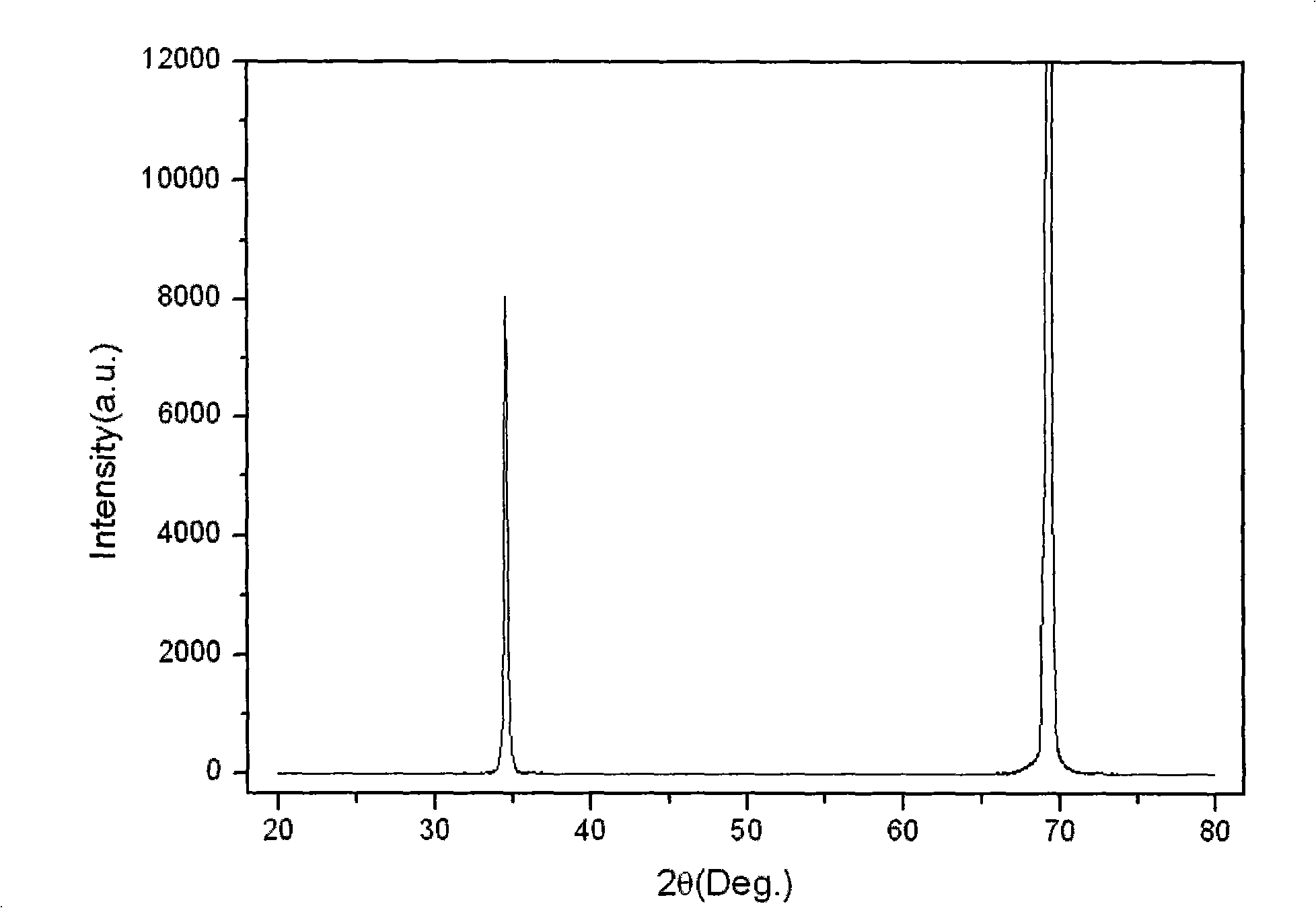
[0025] Utilizing the invention, a p-type ZnO nanowire with a diameter of about 100nm is prepared. X-ray diffraction spectrum shows, only ZnO (002) diffraction peak appears, shows that the As-doped p-type ZnO nanowire that the inventive method makes has good crystalline quality, scanning electron...

Embodiment 2

[0027] Growth of p-type ZnO nanowire arrays with a diameter of about 50 nm

[0028] (1) After weighing the powder of high-purity zinc powder and gallium arsenide according to the mass ratio of 6 / 1, put it into a quartz crucible, and put it into the quartz tube of the chemical vapor deposition system together with the cleaned substrate.

[0029] (3) Vacuumize the quartz tube to below 1000 Pa. When the temperature is heated to 700° C., feed oxygen at a flow rate of 300 ml / min to start the growth of nanowires for 30 minutes.

[0030] (3) After the growth is completed, turn off the oxygen, turn off the heating power, and slowly cool down to below 100°C to take out the sample.

[0031] Utilizing the invention, a p-type ZnO nanowire with a diameter of about 50nm is prepared. X-ray diffraction spectrum shows that the As-doped p-type ZnO nanowires prepared by the inventive method have good crystalline quality, and scanning electron microscopy shows that the prepared ZnO nanowires hav...

Embodiment 3

[0033] The steps of this embodiment and embodiment 1 and embodiment 2 are generally the same, the difference is that zinc arsenide and high-purity zinc powder are used as evaporation sources in the growth process, and other growth conditions are almost the same.


PUM

PropertyMeasurementUnit
lengthaaaaaaaaaa
diameteraaaaaaaaaa
lengthaaaaaaaaaa

Abstract

The invention relates to a method for preparing a p-type ZnO nano-wire, belonging to the semiconductor doping technical field. The invention relates to a doping technology for the p-type ZnO nano-wire, in particular to a doping technology by adoption of the chemical vapor deposition technology and utilization of arsenide as a p-type dopant of ZnO. The doping technology is characterized in that: the doping technology adopts the arsenide as a doping source of the p-type ZnO and utilizes the chemical vapor deposition technology to prepare the arsenic doped p-type ZnO nano-wire. Under the condition that the heating temperature is between 400 and 700 DEG C, the proportion of arsenic doped into the ZnO is controlled by adjusting the mol ratio of the arsenide and zinc, so as to perform growth of the p-type ZnO. The doping technology has the advantages that: the doping technology provides a simple and effective growth technology for preparing the p-tyype ZnO nano-wire with high quality and strong controllability, overcomes the defect of difficult doping of the p-type ZnO nano-wire, and further realizes a p-n junction photoelectric device of the ZnO nano-wire.

Description

technical field [0001] The invention relates to a preparation technology of p-type ZnO nanowires, a method for preparing p-type ZnO nanowires by arsenic doping, which belongs to the field of semiconductor materials, and particularly relates to a chemical vapor deposition method using arsenic compounds as a doping source to carry out p-type ZnO nanowires. A method for preparing ZnO nanowires. Background technique [0002] ZnO is another new type of wide bandgap semiconductor material after GaN, which has higher exciton binding energy than GaN material, and can achieve efficient exciton-related emission at room temperature or even higher temperature. Compared with bulk materials or thin-film materials, ZnO nanowires can further increase the exciton binding energy due to their limited dimensions, making them have more efficient exciton emission performance. In order to realize its application in optoelectronic devices, the doping of p-type ZnO nanowires has become the most imp...

Claims


Application Information

Patent Timeline
Patent Type & Authority Applications(China)
IPC IPC(8): C30B29/16C30B29/62C30B25/00C01G9/02
Inventor 冯秋菊李梦柯宋哲张楠
Owner LIAONING NORMAL UNIVERSITY
Why Eureka
Try Eureka