Method for preparing graphical sapphire substrate for nitrifier epitaxial growth

A sapphire substrate, epitaxial growth technology, applied in the direction of final product manufacturing, sustainable manufacturing/processing, semiconductor/solid-state device manufacturing, etc., can solve the problems of sapphire substrate pollution, complicated process, high cost, etc. Etching damage, low dislocation density, and low cost

Inactive Publication Date: 2008-12-24
INST OF SEMICONDUCTORS - CHINESE ACAD OF SCI
View PDF0 Cites 46 Cited by
  • Summary
  • Abstract
  • Description
  • Claims
  • Application Information

AI Technical Summary

Problems solved by technology

Due to the dry etching equipment involved in the process, the process is complex and t...

Method used


Image

  • Method for preparing graphical sapphire substrate for nitrifier epitaxial growth
  • Method for preparing graphical sapphire substrate for nitrifier epitaxial growth
  • Method for preparing graphical sapphire substrate for nitrifier epitaxial growth

Examples


Embodiment 1

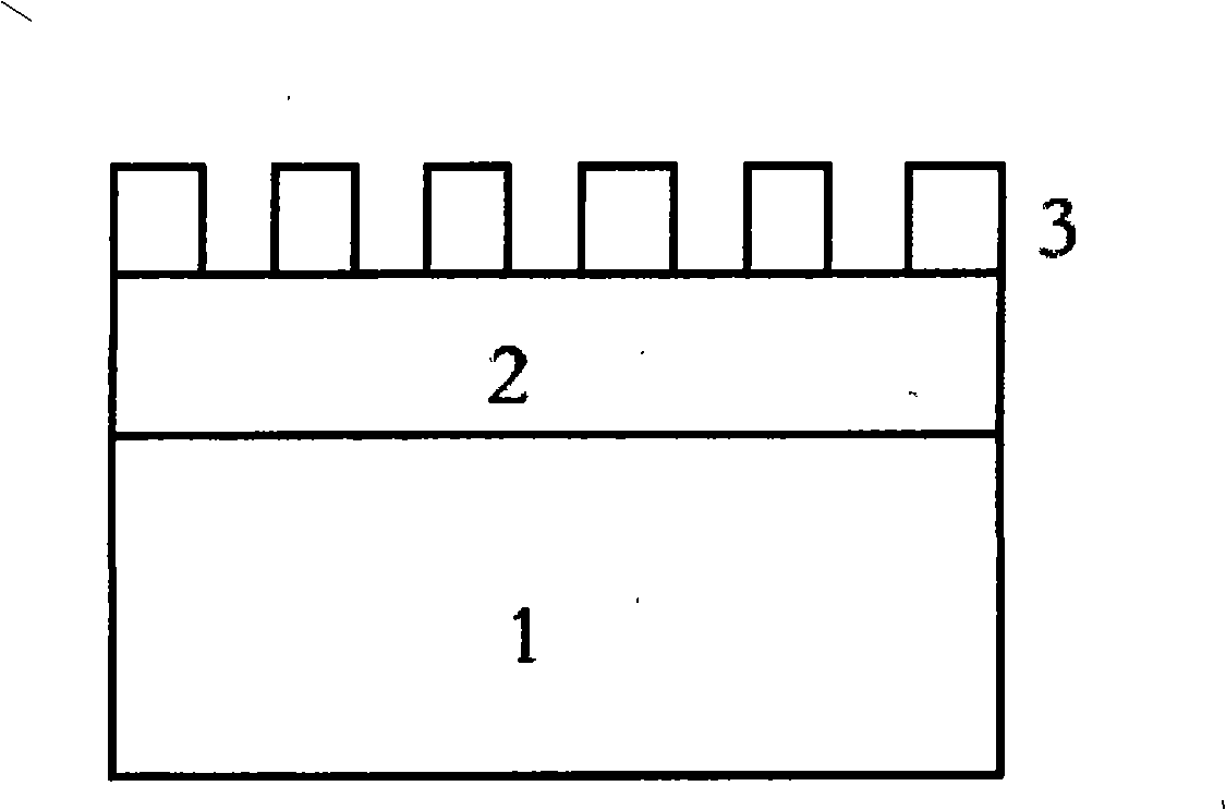
[0032] See again Figure 1-Figure 4 This embodiment is a method for fabricating a patterned c-plane sapphire substrate 1 for nitride epitaxial growth. The c-plane sapphire substrate 1 is currently one of the most commonly used substrate materials for epitaxial growth of nitrides.

[0033] First, a 0.3 micron silicon dioxide film 2 is deposited on a 2-inch c-plane sapphire substrate 1 using plasma enhanced chemical vapor deposition (PECVD) technology, and a photoresist is coated on the silicon dioxide film 2 using conventional photolithography techniques Layer 3 is exposed and developed to form a circular array. The size and pitch of the circular array unit structure is 3 microns, and the structure section after photolithography is as follows figure 1 Shown

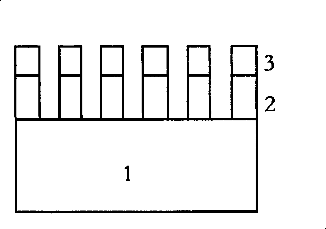
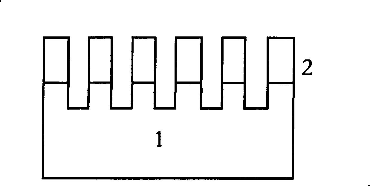
[0034] Then use the photoresist layer 3 as a pattern mask, using hydrofluoric acid (HF) + ammonia fluoride (NH 4 F)+H 2 O mixed solution, etch the photolithography pattern on the silicon dioxide film 2, and its structure secti...

Embodiment 2

[0039] This embodiment is a method for manufacturing a patterned r-plane sapphire substrate 1 for nitride epitaxial growth. The r-plane sapphire substrate 1 can be used for epitaxial growth of non-polar nitrides. Non-polar nitrides can avoid the built-in electric field caused by the strain effect in the vertical growth direction, thereby enhancing the probability of carrier radiation recombination and improving the performance of optoelectronic devices.

[0040]Using a process similar to that of Example 1, a silicon dioxide film is deposited on the r-plane sapphire substrate 1 using plasma-enhanced chemical vapor deposition (PECVD) technology. 2. Conventional lithography technology lithography patterns, hydrofluoric acid (HF )+Ammonia fluoride (NH 4 F)+H 2 The O mixed solution etches the silicon dioxide film 2. The sulfuric acid and phosphoric acid mixture is used to etch the r-face sapphire substrate 1 at 400°C. The etching time is 6 minutes. Finally, the remaining silicon dioxid...


PUM

PropertyMeasurementUnit
Thicknessaaaaaaaaaa

Abstract

The invention discloses a production method of the patterned sapphire substrate for the nitride epitaxial growth, which comprises the following steps: a silica coating is deposited on the sapphire substrate used for the nitride epitaxial growth; a general photetch technology is utilized to prepare a mask of photetch patterns; the photetch patterns are etched on the silica coating by utilizing the doped liquid of hydrofluoric acid, ammonium fluoride and H2O; with the patterned silica coating as a mask, the sapphire substrate are etched by adopting the doped liquid of sulphuric acid and phosphoric acid in a wet manner so that the patterns are etched on the sapphire substrate; a dilute hydrofluoric acid solution is used for wet etching so as to remove the residual silica coating and clean the sapphire substrate, and then the preparation of the patterned sapphire substrate is completed. The production method has the advantages of low cost, preventing the sapphire substrate from being damaged by dry etching, etc. The patterned sapphire substrate can be used for the epitaxial growth of nitrides with low dislocation density and high crystal weight.

Description

Technical field [0001] The invention belongs to the field of semiconductor technology, and particularly refers to a method for manufacturing a patterned sapphire substrate for nitride epitaxial growth. The patterned sapphire substrate can be used for the epitaxial growth of nitride with low dislocation density and high crystal quality. Background technique [0002] Nitride compound semiconductors represented by III-V gallium nitride (GaN), such as gallium nitride (GaN), aluminum nitride (AlN), indium nitride (InN), aluminum gallium nitride (AlGaN), nitrogen Gallium indium (InGaN), aluminum indium nitride (AlInN) or aluminum gallium indium nitride (AlGaInN), etc. are used in ultraviolet / blue / green light-emitting diodes, lasers, solar blind ultraviolet photodetectors, and high-frequency, high-temperature high-power Many fields such as electronic devices have important and extensive applications. At present, the sapphire substrate is the most commonly used substrate for heteroepitax...

Claims


Application Information

Patent Timeline
IPC IPC(8): H01L21/02H01L33/00H01L31/18H01S5/00
CPCY02P70/50
Inventor 闫发旺高海永张扬李晋闽曾一平王国宏张会肖
Owner INST OF SEMICONDUCTORS - CHINESE ACAD OF SCI
Why Eureka
Try Eureka