Manufacturing method of bi-polar transistor array isolated by double shallow slots

A bipolar transistor, shallow trench isolation technology, applied in semiconductor/solid-state device manufacturing, electrical components, circuits, etc., can solve the problems of high manufacturing cost, high manufacturing process, requirements, etc. Effect

Active Publication Date: 2009-01-07
SHANGHAI INST OF MICROSYSTEM & INFORMATION TECH CHINESE ACAD OF SCI
View PDF0 Cites 14 Cited by
  • Summary
  • Abstract
  • Description
  • Claims
  • Application Information

AI Technical Summary

Problems solved by technology

At present, Samsung uses the selective epitaxy method to manufacture bipolar transistors above the heavily doped bit lines, but this method has high requirements on the manufacturing process and the manufacturing cost is very high

Method used


Image

  • Manufacturing method of bi-polar transistor array isolated by double shallow slots
  • Manufacturing method of bi-polar transistor array isolated by double shallow slots
  • Manufacturing method of bi-polar transistor array isolated by double shallow slots

Examples


Embodiment 1

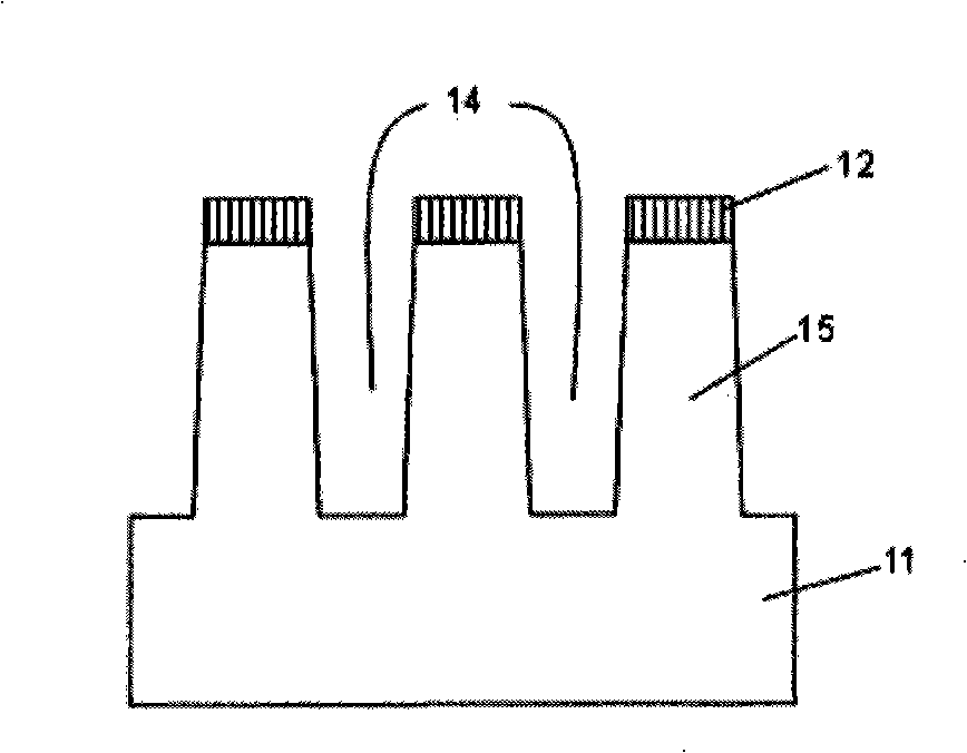
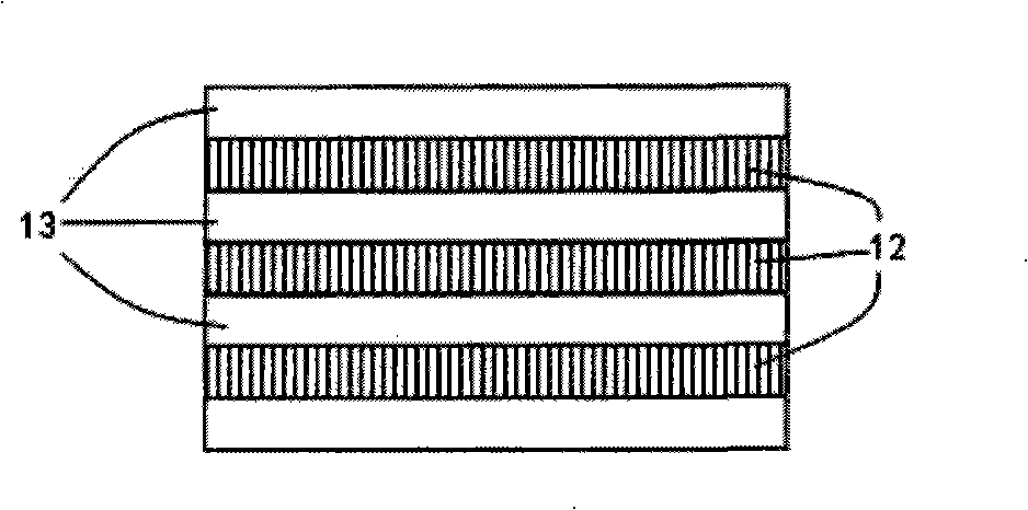
[0039] 1. On a clean p-type conductive substrate 11, an STI groove 14 with a depth of 500 nanometers is manufactured by exposure and etching processes. The part blocked by the photoresist 12 is not etched, and after etching, it is on the silicon wafer Form the protruding lines 15 that are separated from each other; the cross-sectional view of the lines formed after the above-mentioned processing is as Figure 1A As shown, the top view is as Figure 1B shown.

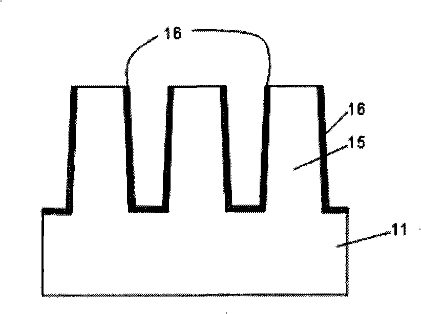
[0040] 2. After removing the glue, use chemical vapor deposition to uniformly deposit the As glass film 16 on the top of the line 15, the side wall and the bottom of the STI groove 14; use chemical mechanical polishing to remove the As-containing glass layer 16 on the line 15. Get the cross-section and top view of the graph such as Figure 1C and Figure 1D shown.

[0041] 3. Spin the photoresist on the above-mentioned substrate with a glue-spinning machine, and the photoresist layer 18 will partly penetrate into the...

Embodiment 2

[0051] A method for manufacturing a bipolar transistor-gated PCRAM device based on the method described above.

[0052] 1. The manufacturing method of manufacturing bipolar transistor array is as embodiment 1.

[0053] 2. Deposit electrode material 24 (TiN 30nm), phase change material 25 (SiSb material 100nm) and electrode material 24 (TiN 30nm) sequentially above the bipolar transistor array obtained above, and manufacture memory cell patterns by photolithography.

[0054] 3. Through the deposition of the dielectric material 29, chemical mechanical polishing and planarization, and then photolithography on the dielectric material, holes are carved in the dielectric material, so that the upper electrode 24 of the phase change memory unit and the bit line 19 are connected by metal plugs 27 and 26 leads out, manufactures electrode 28, forms memory array, as Figure 2A shown. Figure 2A In , the projection along the 5-5 direction is as Figure 2B shown.

Embodiment 3

[0056] 1. On the p-type conductive silicon substrate 30, the STI groove 32 with a depth of 700nm is etched with a photolithography process, and the lines 31 separated from each other are formed, the cross section of which is as follows Figure 3A shown.

[0057] 2. Deposit silicon oxide 33 by vapor phase deposition, such as Figure 3B shown.

[0058] 3. Using the etch-back process, the rest of the silicon oxide at the bottom of the STI groove is etched and removed, such as Figure 3C shown.

[0059] 4. Phosphorus-containing glass 34 is deposited by chemical vapor deposition, adopting a method similar to that of 3 to 5 steps in Example 1 to remove the phosphorus-containing glass at the top and notch of the STI, forming such as Figure 3D The cross-sectional view shown.

[0060] 5. Perform annealing treatment in argon protection, the annealing temperature is 1100 ° C for 5 hours, so that the phosphorus atoms in the material can fully diffuse into the line 31, forming a heavi...


PUM


Abstract

The invention relates to a manufacturing method of a two shallow isolation (dual-STI) bipolar transistor array. The method is characterized in that an selective epitaxial method is avoided in the manufacturing method; a deeper STI is made and formed on a first conductive type underlay; an easy diffused second conductive type atomic materials equably deposit and are contained on the side wall and at the bottom of the STI; the easy diffused second conductive type atomic materials which are deposited near a STI notch are removed. Annealing causes that the second conductive type atomics in the materials to be spread to bit lines, so as to form a second conductive type heavy doping of the bit lines; later, the bit lines which are connected with each other by the diffuse of the second conductive type atomics are separated by etching, so as to ensure that the electricity among bit lines is not communicated; separate bipolar transistors are formed above the separate bit lines by ion injection and photoetching. The transistors on the same bit lines are separated by a lighter STI. The method of the invention also comprises the manufacturing method of a gated phase-change memory based on the two shallow isolation (dual-STI) bipolar transistors.

Description

technical field [0001] The invention relates to a method for manufacturing a double-shallow trench isolation bipolar transistor array, and belongs to the field of phase-change memory manufacturing. Background technique [0002] Phase-change memory (PCRAM) is recognized as the biggest breakthrough in semiconductor memory technology in the past 40 years. It not only has superior performance in all aspects, but also is a general-purpose memory with broad market prospects. After its industrialization, it is expected to partially or completely replace various storage devices including flash (flash memory), DRAM (dynamic random access memory), and hard disk, thereby occupying an important position in the semiconductor memory market. [0003] The storage unit part of the PCRAM is a resistor that can be programmed and adjusted by an electrical signal. In the actual application process, a logic device is required to gate and operate the storage unit. At present, the density of PCRAM...

Claims


Application Information

Patent Timeline
Patent Type & Authority Applications(China)
IPC IPC(8): H01L21/8222H01L21/768H01L21/76
Inventor 张挺宋志棠万旭东刘波封松林陈邦明
Owner SHANGHAI INST OF MICROSYSTEM & INFORMATION TECH CHINESE ACAD OF SCI
Why Eureka
Try Eureka