Method for improving luminous efficiency of GaN based LED by using graphic underlay

A patterned substrate, luminous efficiency technology, applied in the direction of electrical components, circuits, semiconductor devices, etc., can solve the problems that affect the quality of material crystals, limit the photoelectric performance of devices, reduce the efficiency of light extraction, etc., to improve the quality and uniformity of crystals , Improving the internal quantum luminous efficiency and enhancing the effect of light extraction efficiency

Inactive Publication Date: 2009-01-14
YANGZHOU ZHONGKE SEMICON LIGHTING
View PDF0 Cites 49 Cited by
  • Summary
  • Abstract
  • Description
  • Claims
  • Application Information

AI Technical Summary

Problems solved by technology

Due to the large lattice constant mismatch and thermal expansion coefficient difference between the sapphire substrate and the nitride epitaxial layer, there are large residual stress and many crystal defects in the nitride epitaxial layer, which affect the crystal quality of the material and limit the device. Further improvement in optoelectronic performance
At the same time, there is a large difference in refractive index between GaN and air, the light exit angle is very small, and most of it is totally reflected and returned to the inside of the LED device, which not only reduces the light extraction efficiency but also increases the difficulty of heat dissipation, affecting The stability of the LED device

Method used


Image

  • Method for improving luminous efficiency of GaN based LED by using graphic underlay
  • Method for improving luminous efficiency of GaN based LED by using graphic underlay
  • Method for improving luminous efficiency of GaN based LED by using graphic underlay

Examples


Embodiment Construction

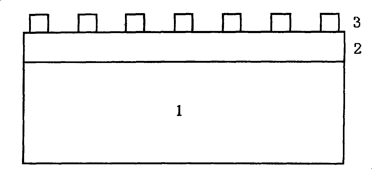
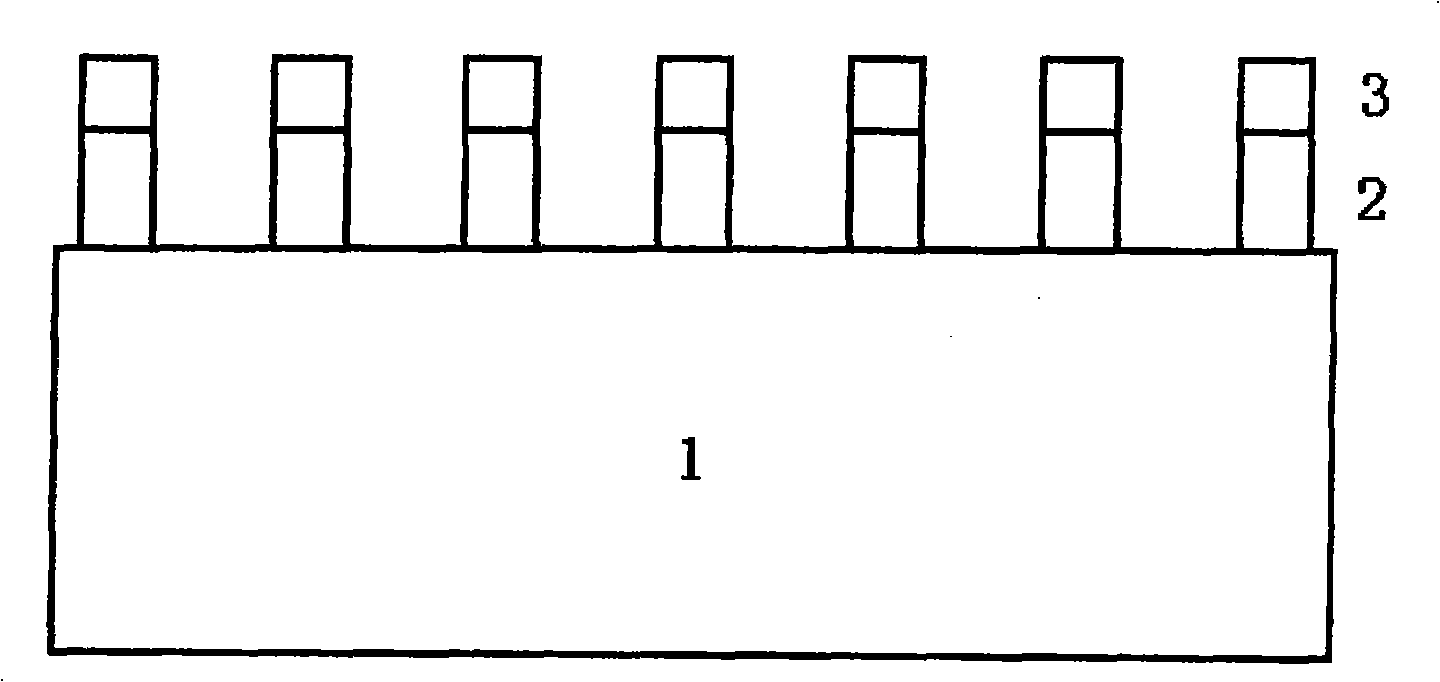
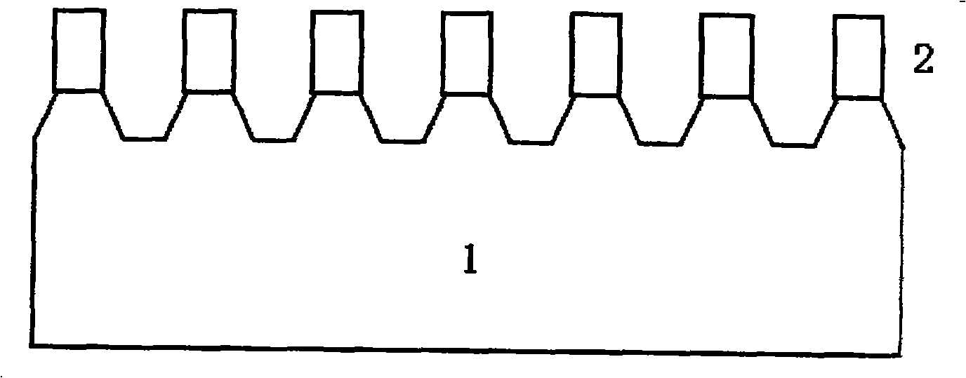
[0032] see Figure 1-Figure 7 As shown, the present invention uses a patterned substrate to improve the method of GaN-based LED luminous efficiency, comprising the following steps:

[0033] Step 1: deposit one layer of silicon dioxide film 2 on sapphire substrate 1 (see figure 1 ), the thickness of the silicon dioxide film 2 is 20 nanometers-2 microns;

[0034] Step 2: using photolithography technology to prepare a photoresist pattern array 3, the pattern unit of which is circular, and the size and pitch of the pattern unit of the circular photoresist pattern array 3 are 0.5 μm-10 μm;

[0035] Step 3: Using the photoresist pattern array 3 as a mask, use hydrofluoric acid + ammonium fluoride + H 2 O mixed solution, etch out the silicon dioxide film 2 with figure structure (referring to figure 2 );

[0036] Step 4: use the silicon dioxide film 2 with pattern structure as a mask, utilize the mixed solution of sulfuric acid and phosphoric acid to etch the sapphire substrate 1...


PUM


Abstract

The invention provides a method which uses a graphic substrate to improve the illumination efficiency of a GaN-based efficiency, comprising the steps as follows: a silicon dioxide film is deposited on a sapphire substrate; a photoresist graphic array is optically etched; the photoresist graphic array is taken as a mask so as to etch the silicon dioxide film with the graphic structure; the silicon dioxide film with the graphic structure is taken as a mask so as to etch the sapphire substrate and the graphics is etched onto the sapphire substrate; the sapphire substrate is thoroughly cleaned so as to form a pyramid structure with triangular sections; a low-temperature nucleation layer grows on the graphic sapphire substrate; temperature is continuously increased on the low-temperature nucleation layer so as to grow an n-typed mixed GaN layer and an array structure which has low dislocation density and V-shaped holes on the surface; a multiple quantum well layer and a p-typed material layer required when the LED structure material grows continue to grow; furthermore, the final surface is led to still have the array structure with V-shaped holes.

Description

technical field [0001] The invention belongs to the technical field of semiconductors, in particular to a method for improving the luminous efficiency of a GaN-based LED by using a patterned substrate. The method can effectively improve the internal quantum luminous efficiency and light extraction efficiency of GaN-based LED materials. Background technique [0002] A light emitting diode (LED) is a junction electroluminescent semiconductor device that converts electrical signals into optical signals. Gallium Nitride (GaN)-based LED, as a solid-state light source, has been hailed as the second revolution in the history of human lighting after Edison invented the electric light for its advantages of high efficiency, long life, and environmental protection. and industry focus. However, GaN-based LEDs are currently entering the field of general lighting, and they still face many difficulties in terms of technology and cost. It is necessary to further improve the internal quant...

Claims


Application Information

Patent Timeline
Patent Type & Authority Applications(China)
IPC IPC(8): H01L33/00
Inventor 闫发旺高永海张扬李晋闽曾一平王国宏张会肖
Owner YANGZHOU ZHONGKE SEMICON LIGHTING
Why Eureka
Try Eureka