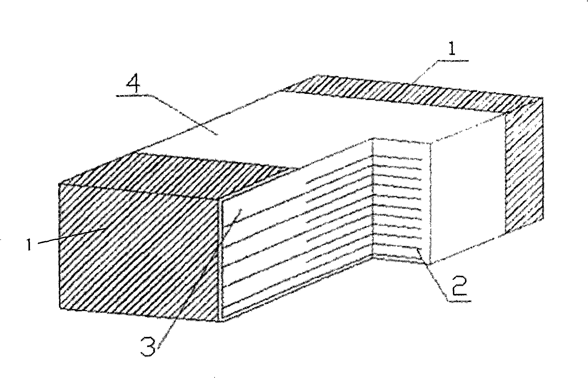
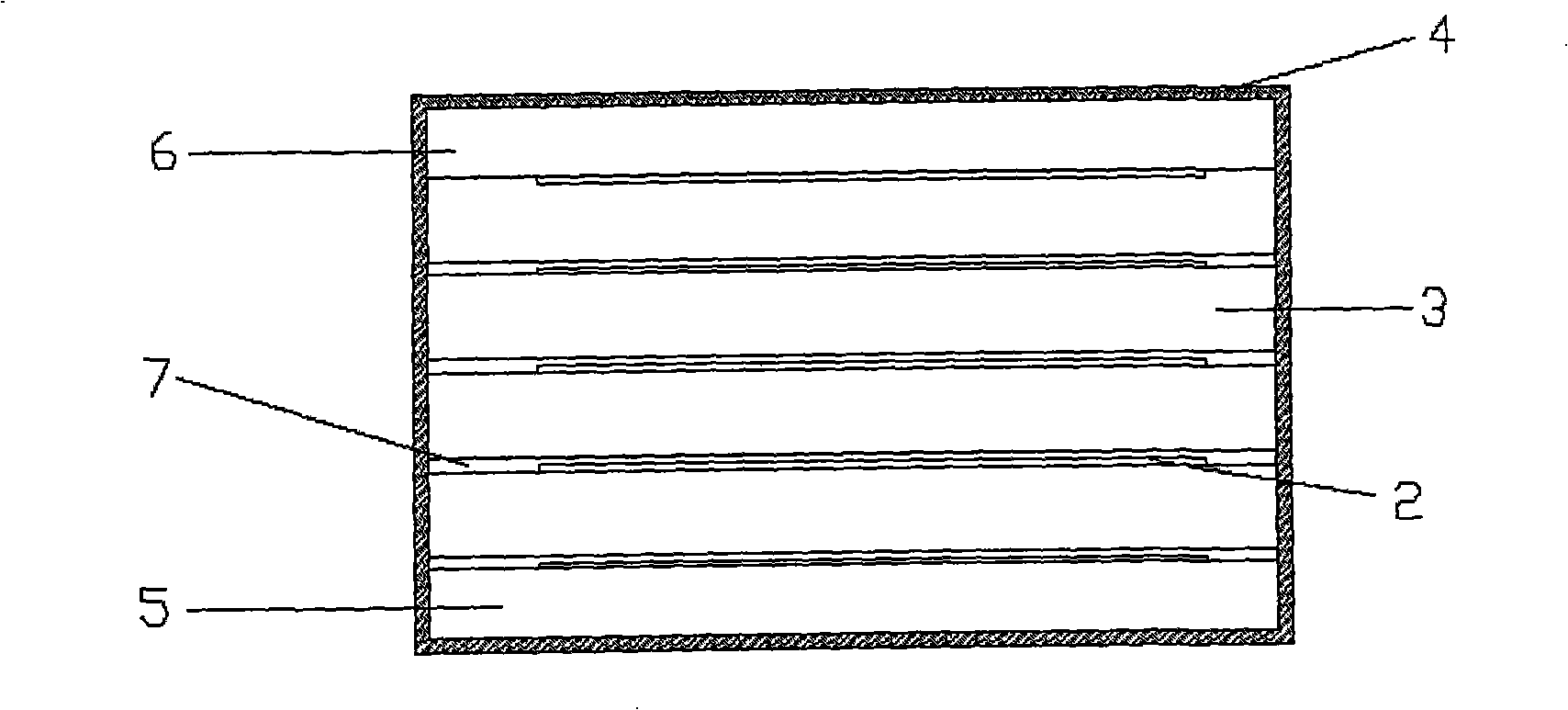
Stacking slice type piezoresistor and manufacturing method thereof
A technology of varistors and varistors, which is applied in varistor cores, resistance manufacturing, varistors, etc., and can solve problems such as high production costs, long production cycles, and difficulty in electroplating nickel and tin treatment , to achieve the effect of shortening the production cycle and saving manufacturing costs
- Summary
- Abstract
- Description
- Claims
- Application Information
AI Technical Summary
Problems solved by technology
Method used
Image

Examples
Embodiment 1
[0057] The manufacturing method of the piezoresistor provided by the embodiment of the present invention comprises the following steps:
[0058] (1) Powder preparation:
[0059] The varistor film material was ground and mixed uniformly for 20 hours until the particle size was 1.0 μm, dried at 150°C, and sieved with 80 mesh. The material components and their weight percentages were:
[0061] Bismuth oxide Bi 2 o 3 3.5%
[0062] Antimony oxide Sb 2 o 3 5%
[0063] Cobalt oxide Co 3 o 4 2%
[0064] Manganese Carbonate MnCO 3 0.5%
[0065] Chromium oxide Cr 2 o 3 1%
[0066] Nickel oxide Ni 2 o 3 1%
[0067] Aluminum nitrate Al(NO 3 ) 3 9H 2 O 0.01%
[0068] Silver nitrate AgNO 3 0.02%
[0069] boric acid H 2 BO 3 1%
Embodiment 2
[0093] (1) Powder preparation:
[0094] The varistor film material was ground and mixed uniformly for 20 hours until the particle size was 1.0 μm, dried at 150°C, and sieved with 80 mesh. The material components and their weight percentages were:
[0095] Grind and uniformly mix the ceramic protective layer material for 20 hours until the particle size is 1.0 μm, dry at 150°C, and sieve through 80 mesh. The material components and their weight percentages are:
[0097] Silicon oxide SiO 2 50%
[0098] Bismuth oxide Bi 2 o 3 8%
[0099] Boron oxide B 2 o 3 12%
[0100] Alumina Al2 o 3 15%
[0102] Magnesium Oxide MgO 2.5%
[0103] Manganese Carbonate MnCO 3 3%
[0104] (2) configure the slurry: configure the slurry with the above-mentioned powder ratio, and the method is the same as in Example 3.
[0105] (3) Tape mak...
PUM
| Property | Measurement | Unit |
|---|---|---|
| Thickness | aaaaa | aaaaa |
| Thickness | aaaaa | aaaaa |
| Thickness | aaaaa | aaaaa |
Abstract
Description
Claims
Application Information
 - Generate Ideas
- Intellectual Property
- Life Sciences
- Materials
- Tech Scout
- Unparalleled Data Quality
- Higher Quality Content
- 60% Fewer Hallucinations
Browse by: Latest US Patents, China's latest patents, Technical Efficacy Thesaurus, Application Domain, Technology Topic, Popular Technical Reports.
© 2025 PatSnap. All rights reserved.Legal|Privacy policy|Modern Slavery Act Transparency Statement|Sitemap|About US| Contact US: help@patsnap.com