Method for making fully self-aligning bar gate power vertical bilateral diffusion field-effect tranisistor

A field-effect transistor, vertical double diffusion technology, applied in semiconductor/solid-state device manufacturing, electrical components, circuits, etc., can solve problems such as the reduction of unfavorable chip area, the increase of operating frequency, and the complex process, so as to reduce the production cost. , The effect of increasing the contact hole area and simplifying the manufacturing process

Active Publication Date: 2009-04-01
SEMICON MFG INT (SHANGHAI) CORP +1
View PDF0 Cites 14 Cited by
  • Summary
  • Abstract
  • Description
  • Claims
  • Application Information

AI Technical Summary

Problems solved by technology

However, in order to form a good metal contact with the P-well and N+ source, two photolithography masks (P-well contact injection mask, N+ source injection mask) are usually required, and a total of 7 to 9 masks are required. , which is not conduc...

Method used


Image

  • Method for making fully self-aligning bar gate power vertical bilateral diffusion field-effect tranisistor
  • Method for making fully self-aligning bar gate power vertical bilateral diffusion field-effect tranisistor
  • Method for making fully self-aligning bar gate power vertical bilateral diffusion field-effect tranisistor

Examples


Embodiment Construction

[0044] In order to make the object, technical solution and advantages of the present invention clearer, the present invention will be described in further detail below in conjunction with specific embodiments and with reference to the accompanying drawings.

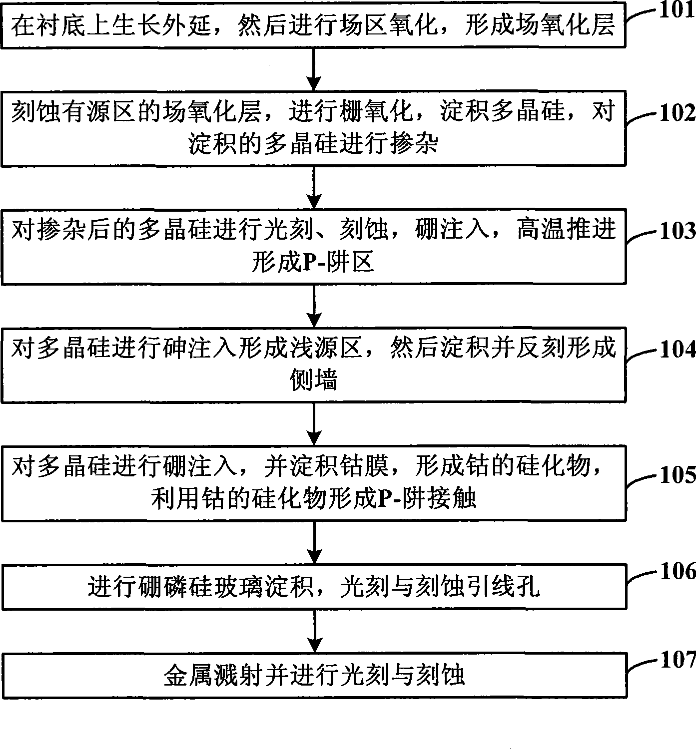
[0045] Such as figure 1 as shown, figure 1 A flow chart of a method for making a fully self-aligned strip gate power DMOS transistor provided by the present invention, the method includes the following steps:

[0046] Step 101: growing epitaxy on the substrate, and then performing field oxidation to form a field oxide layer;

[0047] Step 102: etching the field oxide layer of the active region, performing gate oxidation, depositing polysilicon, and doping the deposited polysilicon;

[0048] Step 103: performing photolithography and etching on the doped polysilicon, implanting boron, and advancing at high temperature to form a P-well region;

[0049] Step 104: performing arsenic implantation on the polysilicon to form a...


PUM


Abstract

The invention relates to the technical field of semiconductor device and integrated circuit fabrication technologies and discloses a method for preparing a DMOS power transistor with a fully self aligned strip-type gate. The method comprises: A. epitaxial growth is carried out on a substrate, and a field area is oxidized thereafter, thereby forming a field oxide layer; B. the field oxide layer in active area is etched, a gate region is oxidized, then, amorphous silicon is deposited, and the deposited amorphous silicon is doped thereafter; C. lithography, etching and boron injection are carried out on the amorphous silicon after being doped, and the injected boron is pushed forward under high temperature, thereby forming a P-type well region; D. the amorphous silicon is injected with arsenic to form a shallow source region, and then a side wall is formed by deposition and anti-etching; E. boron is injected into the amorphous silicon, a cobalt film is deposited, and then cobalt silicide is formed, and P-type well contact is formed by making use of the cobalt silicide; F. boron-phosphorosilicate glass is deposited, and pulling holes are formed by lithography and etching; G. metal is deposited by sputtering, and lithography and etching are carried out thereafter. The invention simplifies the fabrication process, reduces the fabrication cost and improves the operating frequency of the DMOS power transistor.

Description

technical field [0001] The invention relates to the technical field of semiconductor devices and integrated circuit manufacturing technology, in particular to a method for manufacturing a fully self-aligned strip gate power vertical double-diffusion field-effect transistor (VerticalDouble-diffusion MOSFET, DMOS). Background technique [0002] Power DMOS transistors have been widely used in various electronic devices. Power DMOS transistors have the characteristics of fast switching speed, high input impedance, low driving power consumption, good frequency characteristics, highly linear transconductance, etc., and have a negative temperature coefficient, no secondary breakdown problem of bipolar power transistors, and a large safe working area . Therefore, whether it is a switching application or a linear application, DMOS transistors are ideal power devices. [0003] In the traditional power DMOS transistor manufacturing process, the polysilicon boundary is used as the ali...

Claims


Application Information

Patent Timeline
IPC IPC(8): H01L21/8234H01L21/336
Inventor 王立新
Owner SEMICON MFG INT (SHANGHAI) CORP
Why Eureka
Try Eureka