

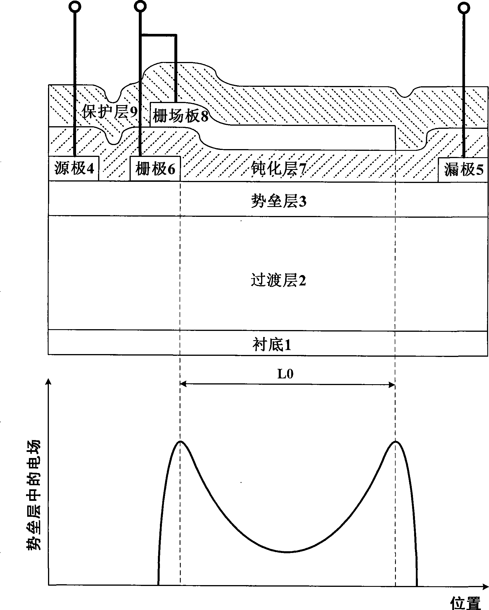
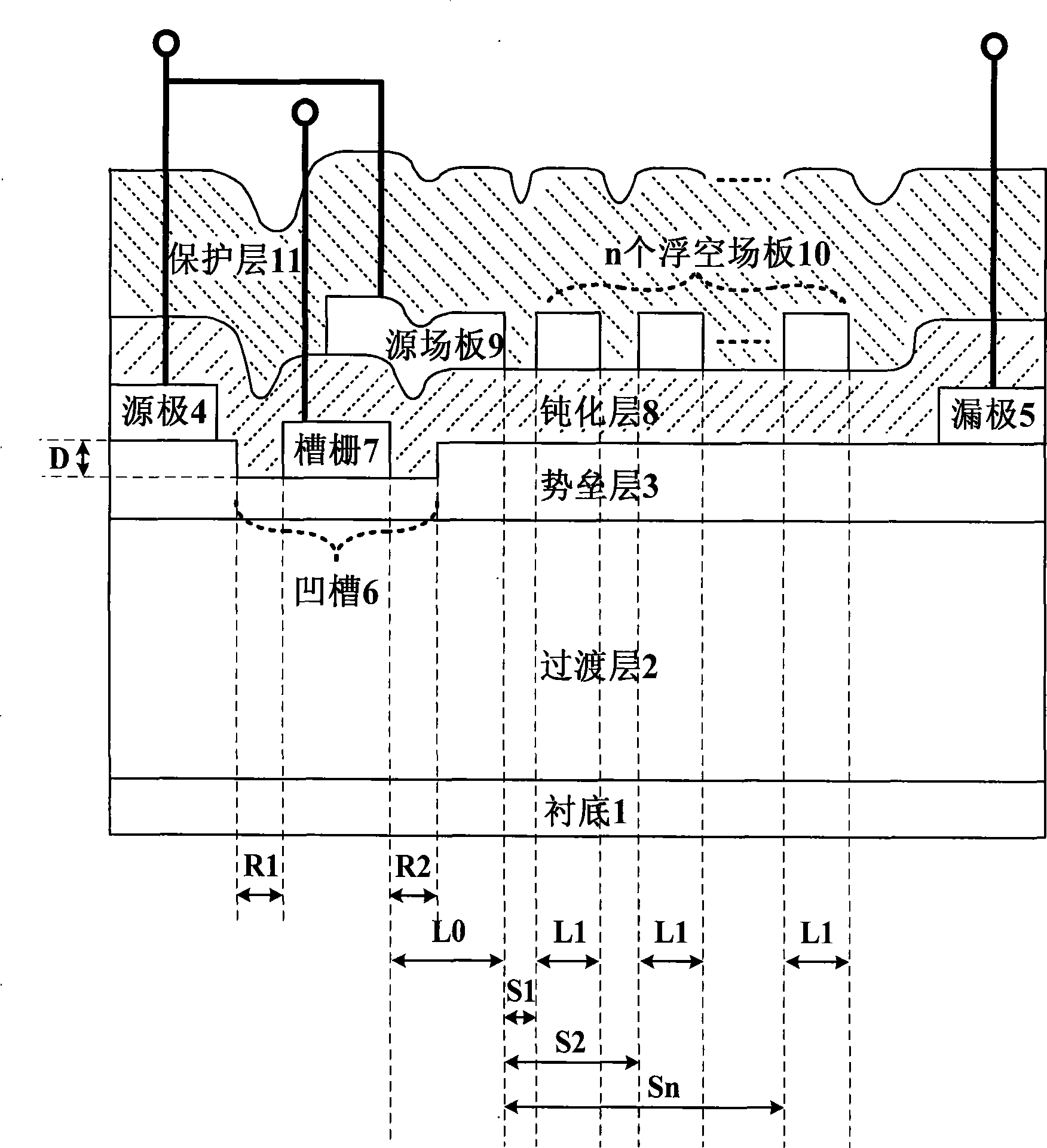
High electron mobility device for trench gate type source field board and manufacturing method therefor
A high electron mobility, source field plate technology, applied in the field of microelectronics, can solve the problems of reducing the yield of the device, complicated manufacturing process, tedious process debugging, etc., and achieve the effect of reducing the electric field, improving the breakdown voltage and enhancing the reliability.
- Summary
- Abstract
- Description
- Claims
- Application Information
AI Technical Summary
Problems solved by technology
Method used
Image

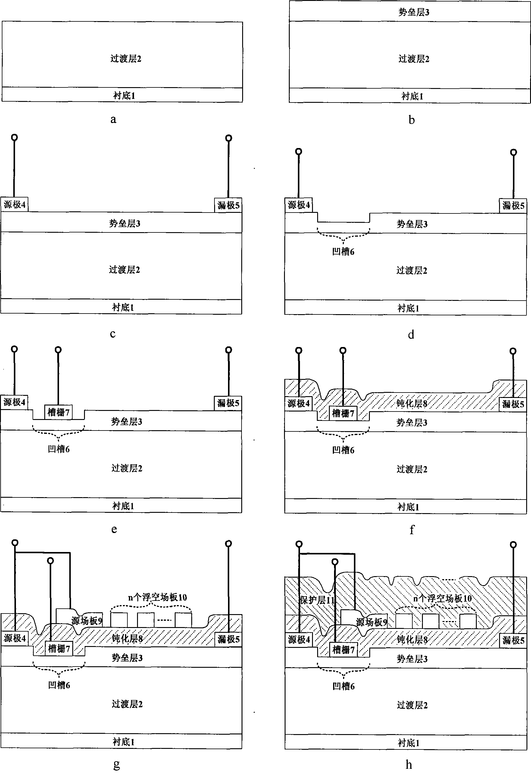
Examples
Embodiment 1
[0057] The production substrate is sapphire, and the passivation layer is SiO 2 , the protective layer is SiN, the source field plate and each floating field plate are Ti / Au metal combination groove gate type source field plate high electron mobility device, the process is:
[0058] 1. Using metal organic chemical vapor deposition technology to epitaxially undoped transition layer 2 with a thickness of 1 μm on the sapphire substrate 1, the transition layer is composed of AlN material with a thickness of 22 nm and GaN material with a thickness of 0.978 μm from bottom to top constitute. The process conditions used for the epitaxial lower layer AlN material are: temperature 565°C, pressure 40 Torr, hydrogen gas flow rate 4200 sccm, ammonia gas flow rate 4200 sccm, aluminum source flow rate 20 μmol / min; the process conditions for the epitaxial upper layer GaN material are: temperature 950°C, the pressure is 40 Torr, the flow rate of hydrogen gas is 4200 sccm, the flow rate of amm...
Embodiment 2
[0067] The production substrate is silicon carbide, the passivation layer is SiN, and the protective layer is SiO 2 , the source field plate and each floating field plate are Ni / Au metal combined groove gate type source field plate high electron mobility device, the process is:
[0068] 1. Use metal organic chemical vapor deposition technology to epitaxially have an undoped transition layer 2 with a thickness of 2.5 μm on a silicon carbide substrate 1. The transition layer is composed of an AlN material with a thickness of 50 nm and an AlN material with a thickness of 2.45 μm from bottom to top. Made of GaN material. The process conditions used for the epitaxial lower layer AlN material are: temperature 1020°C, pressure 45 Torr, hydrogen gas flow rate 4800 sccm, ammonia gas flow rate 4800 sccm, aluminum source flow rate 12 μmol / min; the process conditions for the epitaxial upper layer GaN material are: temperature 1020°C, the pressure is 45 Torr, the flow rate of hydrogen gas...
Embodiment 3
[0077] The production substrate is silicon, and the passivation layer is Al 2 o 3 , the protective layer is SiN, the source field plate and each floating field plate are Pt / Au metal combination groove gate type source field plate high electron mobility device, the process is:
[0078] 1. Using metal organic chemical vapor deposition technology to epitaxially undoped transition layer 2 with a thickness of 5 μm on the silicon substrate 1, the transition layer is composed of AlN material with a thickness of 125 nm and GaN material with a thickness of 4.875 μm from bottom to top constitute. The process conditions used for the epitaxial lower layer AlN material are: temperature 860 °C, pressure 50 Torr, hydrogen gas flow rate 4900 sccm, ammonia gas flow rate 4900 sccm, aluminum source flow rate 35 μmol / min; the process conditions used for the epitaxial upper layer GaN material are: temperature 1050°C, pressure 50 Torr, hydrogen gas flow rate 4900 sccm, ammonia gas flow rate 4900 ...
PUM
 Abstract
Description
Claims
Application Information