Glass passivating technique process for semi-conductor device with silicon large diameter round wafer

A glass passivation and large-diameter technology, which is applied in semiconductor/solid-state device manufacturing, electrical components, circuits, etc., can solve problems affecting long-term working life, difficulty in overall planning, power device reduction of power indicators, etc., to achieve electrical parameters and reliability Performance optimization, simple technical method and remarkable effect

Inactive Publication Date: 2009-06-17
林楠
View PDF0 Cites 8 Cited by
  • Summary
  • Abstract
  • Description
  • Claims
  • Application Information

AI Technical Summary

Problems solved by technology

However, the above measures still have major shortcomings, mainly: even if the glass formula is improved under the premise of ensuring the glass passivation effect, it is difficult to achieve a complete match between the thermal expansion coefficient of glass and silicon and the uniformity of this match with temperature changes ; In the process of glass passivation thermoforming, it is necessary to optimize the reverse characteristics of the device and at the same time minimize the internal stress of glass-silicon. The two are not unified under the same heat treatment conditions, so it is difficult to coordinate Taking into account; intentionally leaving a thick silicon substrate when thinning the back is not conducive to heat dissipation of the device, which will increase the junction temperature of the device during operation and affect the long-term working life. For power devices, the key power indicators will be significantly reduced, while for radio frequency For the device, it will significantly increase the high-frequency loss; the above methods are still difficult to solve various drawbacks in internal stress, electrical performance or reliability

Method used


Image

  • Glass passivating technique process for semi-conductor device with silicon large diameter round wafer

Examples


Embodiment 1

[0020] Embodiment 1 Silicon switch diode glass passivation technology and method

[0021] Silicon substrate diameter: 3 inches

[0022] Original thickness of silicon wafer: 480μm

[0023] Chip size on silicon substrate: mesa height 30μm~35μm

[0024] Mesa diameter Φ45μm~Φ50μm

[0025] The distance between adjacent chips is 350μm

[0026] P + N - Junction depth 5μm~5.5μm

[0027] N-layer thickness 24μm~25μm

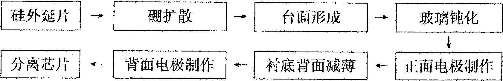
[0028] Process steps:

[0029] 1. Strict chemical cleaning and drying of the silicon wafers etched on the device table;

[0030] 2. Fabricate glass passivation film by scraping method, and in P + Open the electrode contact window on the surface to make the front electrode system;

[0031] 3. Use a grinding wheel dicing machine with a knife width of 10-20 μm, and the depth of the knife is 35 μm for the height of the table, and cut the glass film groove between the adjacent chips on the...

Embodiment 2

[0034] Embodiment 2 Silicon varactor glass passivation technology method

[0035] Silicon substrate diameter: 3 inches

[0036] Original thickness of silicon wafer: 480μm

[0037] Chip size on silicon substrate: mesa height 8μm~10μm

[0038] Mesa diameter Φ105μm~Φ110μm

[0039] The distance between adjacent chips is 350μm

[0040] P + N - Junction depth 0.6μm~0.8μm

[0041] N-layer thickness 2μm~2.5μm

[0042] Process steps:

[0043] 1. Strict chemical cleaning and drying of the silicon wafers etched on the device table;

[0044] 2. Make glass passivation film by scraping method;

[0045] 3. Use a photolithography mask with a line width of 15 μm and an outer frame size of 365 μm×365 μm to carve a glass film layer groove with a strip width of about 25 μm between adjacent chips, subject to the engraved clean glass film;

[0046] 4. In P + The electrode contact window is opened on the surfa...

Embodiment 3

[0049] Example 3 Glass Passivation Technology and Method of Silicon Pin ESC Attenuation Diode

[0050] Silicon substrate diameter: 3 inches

[0051] Original thickness of silicon wafer: 480μm

[0052] Chip size on silicon substrate: Mesa diameter Φ90μm~Φ95μm

[0053] Mesa height 110μm~115μm

[0054]The distance between adjacent chips is 400μm

[0055] P + N - Junction depth 5μm~5.5μm

[0056] N-layer thickness 70μm~80μm

[0057] Process steps:

[0058] 1. Strict chemical cleaning and drying of the silicon wafers etched on the device table;

[0059] 2. Use a box-shaped screen printing mask with a line width of 20 μm and an outer frame size of 420 μm×420 μm. The real part of the mask covers the centerline of the adjacent die, and the imaginary part of the mask exposes the device chip for passivation protection. area;

[0060] Apply the glass paste by scraping method, remove the mask after drying to thermofo...


PUM

PropertyMeasurementUnit
diameteraaaaaaaaaa
diameteraaaaaaaaaa
diameteraaaaaaaaaa

Abstract

A glass passivation technique for large-diameter silicon wafer semiconductor devices is characterized by utilizing cutting and photoetching processes to isolate a passivating glass film layer between chips on a silicon substrate before thinning the back surface of the substrate of the large-diameter silicon wafer, or utilizing a screen mask isolating process to isolate the passivating glass film layer between the chips on the silicon substrate during glass passivation. Glass-silicon internal stress caused by difference of passivating glass-silicon thermal expansion coefficients in the glass passivation process can be effectively released or eliminated in a small range among chips, thereby effectively preventing silicon wafer warping, cracking or breaking caused by thinning the back surface of the substrate of the large-diameter silicon wafer. The technique can guarantee realization of the optimum designs of electric parameters and reliability for silicon semiconductor devices during glass passivation, and is particularly adaptable to large scale production of glass-passivated semiconductor devices with large-diameter silicon wafers.

Description

Technical field: [0001] The invention belongs to the technical field of surface passivation of semiconductor devices, and is mainly applied to the surface passivation of silicon semiconductor devices. Background technique: [0002] In the glass passivation process technology of semiconductor devices, there are mainly two types of passivation glass currently used, namely, lead-based passivation glass and zinc-based passivation glass. The electrical, chemical, and thermal properties required by semiconductor devices should be met in order to ensure the processability of the process and the electrical performance and reliability of the passivated device. [0003] The originally developed glass passivation technology is mainly used in low-frequency and high-power semiconductor devices. Although the composition of the passivation glass has been carefully designed, there is always a difference in the thermal expansion coefficient of glass and silicon during the thermoforming proce...

Claims


Application Information

Patent Timeline
Patent Type & Authority Applications(China)
IPC IPC(8): H01L21/02
Inventor 林楠
Owner 林楠
Why Eureka
Try Eureka