

Electric pumping silicon base MgxZn1-xO film ultraviolet accidental laser and preparation method thereof
A random laser, mgxzn1-xo technology, applied in the direction of lasers, laser parts, laser parts, etc., to achieve the effect of simple structure and implementation
- Summary
- Abstract
- Description
- Claims
- Application Information
AI Technical Summary
Problems solved by technology
Method used
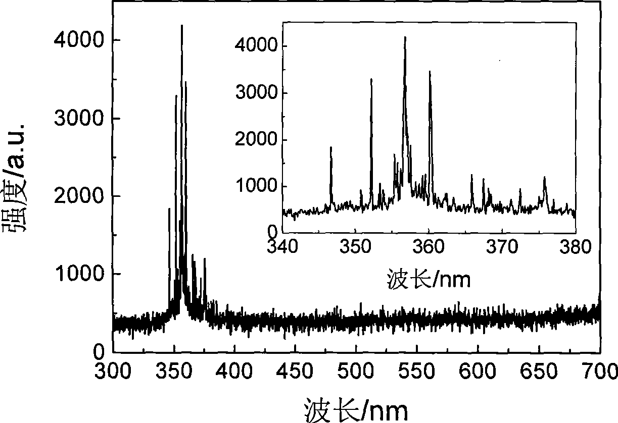
Image

Examples
Embodiment 1
[0023] Take the following process steps:
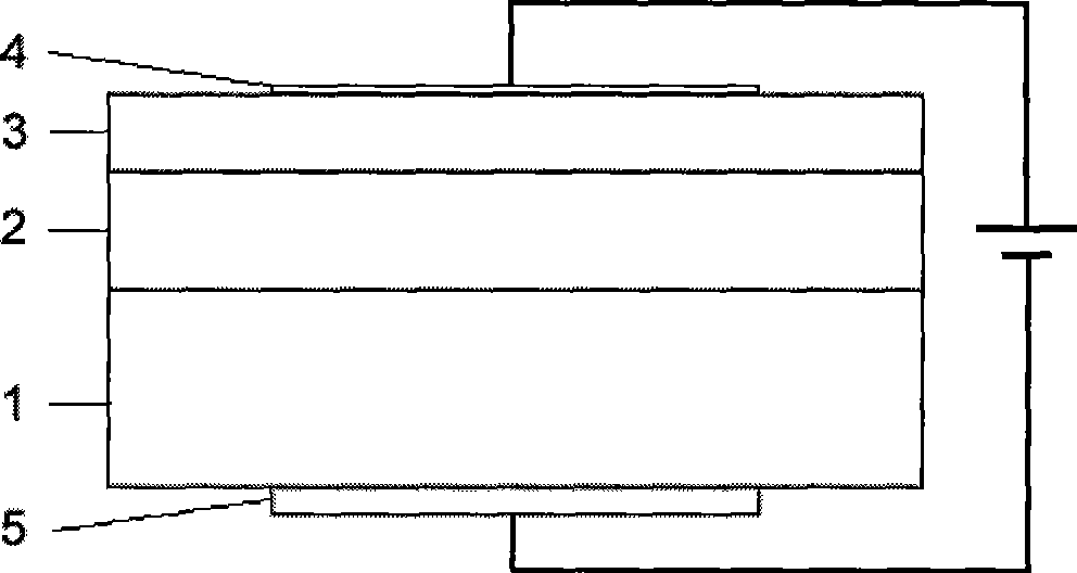
[0024] 1) Clean n-type , resistivity 0.005 ohm cm, size 15×15mm 2 , a silicon wafer with a thickness of 675 microns, after cleaning, put it into the reaction chamber of the DC reactive magnetron sputtering device, and the vacuum degree of the reaction chamber is pumped to 1×10 -3 Pa; Deposit Mg with a thickness of about 300 nm on a silicon wafer by DC reactive magnetron sputtering x Zn 1-x O(x=0.2) film, when sputtering, use Mg 0.2 Zn 0.8 Alloy target, substrate temperature 300°C, sputtering power 80W, pass through O 2 Mixed gas with Ar, O 2 The flow ratio to Ar is 1:2, and the working pressure is 10Pa;
[0025] 2) Using alumina powder as the evaporation source, the Mgx Zn 1-x An aluminum oxide film with a thickness of about 100 nm is deposited on the O (x=0.2) film;
[0026] 3) Sputter 20nm and 100nm thick Au films on the aluminum oxide film and the back of the silicon substrate respectively, wherein the area of the former ...
Embodiment 2
[0029] Take the following process steps:
[0030] 1) Clean N-type , with a resistivity of 0.5 ohm cm and a size of 15×15mm 2 , a silicon wafer with a thickness of 675 microns; according to the chemical formula Mg 0.25 Zn 0.75 , zinc acetate (Zn(Ac) 2 2H 2 O) and magnesium acetate (Mg(Ac) 2 4H 2 O) be dissolved in ethylene glycol methyl ether solution, and add ethanolamine as stabilizer, stir to obtain Mg 0.25 Zn 0.75 O precursor solution (the sum of the concentrations of Zn and Mg in the solution is 1.2M, and the molar ratio Zn:Mg=3:1), and then use the sol-gel method to spin-coat the silicon wafer with a thickness of about 400nm. Mg x Zn 1-x O(x=0.25) film, dried at 100°C for 20 minutes after spin-coating, and then heat-treated at 800°C for 2 hours under oxygen;
[0031] 2) Using silicon nitride ceramics as the target material, Mg x Zn 1-x Deposit a silicon nitride film with a thickness of about 100nm on the O(x=0.25) film. During sputtering, the substrate tempera...
Embodiment 3
[0036] Take the following process steps:
[0037] 1) Clean N-type , the resistivity is 50 ohm cm, and the size is 15×15mm 2 , a silicon wafer with a thickness of 675 microns; according to the chemical formula Mg 0.35 Zn 0.65 , zinc acetate (Zn(Ac) 2 2H 2 O) and magnesium acetate (Mg(Ac) 2 4H 2 O) be dissolved in ethylene glycol methyl ether solution, and add ethanolamine as stabilizer, stir to obtain Mg 0.35 Zn 0.65 O precursor solution (the sum of the concentrations of Zn and Mg in the solution is 1.2M, and the molar ratio Zn:Mg=13:7), and then use the sol-gel method to spin-coat the silicon wafer with a thickness of about 400nm. Mg x Zn 1-x O(x=0.35) film, after spin-coating, dry at 100°C for 20 minutes, then heat-treat at 800°C for 2 hours under oxygen;
[0038] 2) Using quartz powder as the evaporation source, the Mg x Zn 1-x A silicon oxide film with a thickness of about 100 nm is deposited on the O(x=0.35) film;
[0039] 3) Sputter deposit a 30nm thick Au fi...
PUM
 Abstract
Description
Claims
Application Information