Schottky type nuclear battery and preparation method thereof
A Schottky-type, nuclear battery technology, applied in circuits, nuclear engineering, electrical components, etc., can solve the problems of inability to meet long-term power supply, small battery energy volume, etc., to improve energy conversion efficiency, improve energy density, and prolong use. effect of life
- Summary
- Abstract
- Description
- Claims
- Application Information
AI Technical Summary
Problems solved by technology
Method used
Image
Examples
Embodiment 1
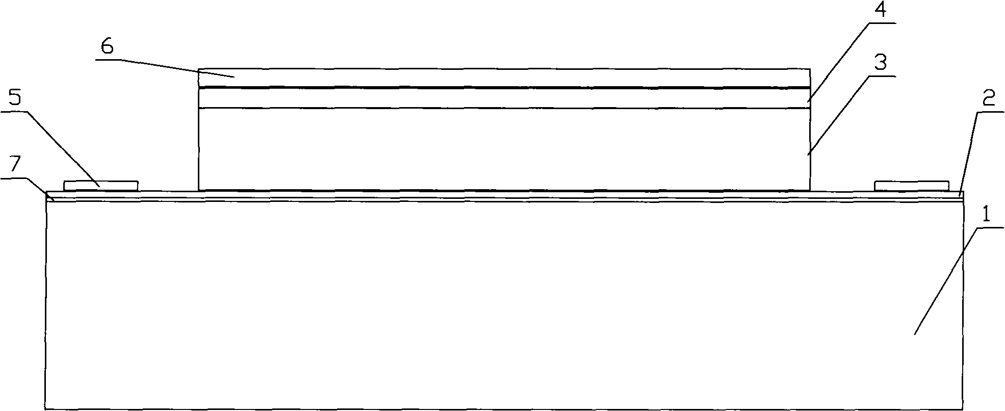
[0027] Such as figure 1 The shown schematic diagram of the structural axis section of an embodiment of the nuclear battery, first prepare the Al 2 o 3 Wafers, which can be purchased from the market to obtain single-side polished 2-inch C-side β-Al 2 o 3 The substrate 1 has a thickness of 300 μm.
[0028] Then perform the Schottky wafer growth process: use MOCVD epitaxial growth equipment, first Al 2 o 3 Substrate 1 is nitrided by passing through ammonia gas at 1100°C for about 2 minutes, then cooling down to 570°C, passing through trimethylgallium and ammonia gas to epitaxially form a gallium nitride (GaN) buffer layer 7 of about 20nm, and then raising the temperature to 1150°C Controlling the silicon doping concentration at 1×10 18 / cm 3 Under stable conditions, trimethylgallium, ammonia gas and silane are introduced to epitaxy n-GaN doped layer 2 of about 2 μm, and then the sample is taken out after cooling down to room temperature; Ammonia gas and metal gallium epit...
Embodiment 2
[0031] Prepare Al first 2 o 3 Wafers, which can be purchased from the market to obtain single-side polished 2-inch C-side β-Al 2 o 3 The substrate 1 has a thickness of 400 μm.
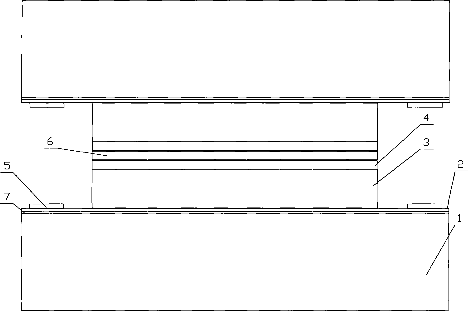
[0032] Then perform the Schottky wafer growth process: use MOCVD epitaxial growth equipment, first raise the temperature to 1150°C and control the silicon doping concentration at 1×10 19 / cm 3 Under stable conditions, trimethylgallium, ammonia gas and silane are introduced to epitaxy n-GaN doped layer 2 of about 2 μm, and then the sample is taken out after cooling down to room temperature; Ammonia gas and metal gallium epitaxy a 20 μm GaN insulating layer 3 , and then lowered to room temperature, and samples were taken out.
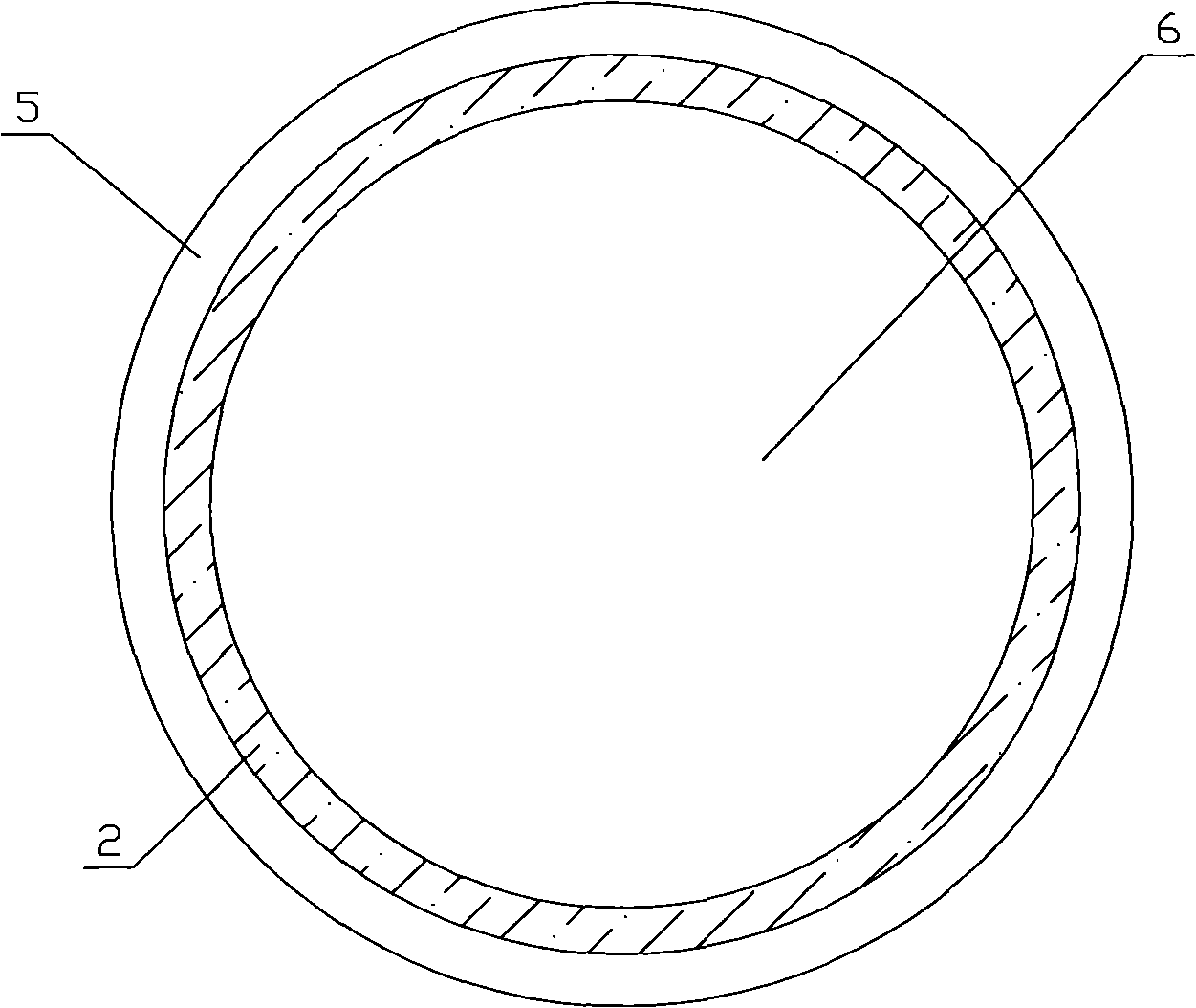
[0033]Next, use ultraviolet lithography machine photolithography and ICP etching technology, obtain n-type steps on the surface of n-type GaN doped layer 2; Use magnetron sputtering technology to deposit Ti (20nm) / Al ( 20nm) / Ti(20nm) / Au(300nm) (i.e. Ti deposition 20nm, Al de...
Embodiment 3
[0036] The preparation method is the same as that of the above two examples. The battery structure can be either the single structure of Example 1 or the composite structure of Example 2. The difference of this example is that the isotope layer 6 can also use nuclear waste strontium-90 , can also realize the preparation of high-efficiency radiovoltaic effect nuclear battery.
[0037] It should be noted that in all implementations including the above three examples, the thickness of the Schottky contact electrode cannot exceed 40nm (calculated on one side for the situation described in Example 2), otherwise it will affect the nuclear battery. conversion efficiency. Moreover, different nuclear batteries can be integrated in a certain way to obtain higher voltage or current nuclear batteries to meet the needs of different situations.
[0038] From the point of view of expanding applications, the micro-energy layout (each nuclear cell is a circular surface with a diameter of 200 ...
PUM
 Abstract
Description
Claims
Application Information


