Method for preparing double side dielectric groove part SOI material

A dielectric groove and double-sided technology, which is applied in the field of material preparation of SOI power devices, can solve the problems of low withstand voltage, easy breakdown in advance, and low withstand voltage of SOI devices, so as to ensure the quality of SiO2, reduce self-heating effect, and withstand high voltage The effect of heat dissipation

Inactive Publication Date: 2009-09-09
UNIV OF ELECTRONICS SCI & TECH OF CHINA
View PDF1 Cites 8 Cited by
  • Summary
  • Abstract
  • Description
  • Claims
  • Application Information

AI Technical Summary

Problems solved by technology

However, this structure does not completely solve the problem of low withstand voltage of SOI devices. This is because, first, the electric field of the buried oxide layer does not increase significantly, σ S =0, the electric field E of the buried oxide layer I ≈3E S ; Second, the thickness of the buried oxide layer is 20-100nm, and the thickness of the top silicon layer is 20-300nm. According to formulas (1) and (2), the withstand voltage of the device is lower than 100V
Third, the structure has no buried oxide layer only at the source end away from the channel region, and the substrate si...

Method used


Image

  • Method for preparing double side dielectric groove part SOI material
  • Method for preparing double side dielectric groove part SOI material
  • Method for preparing double side dielectric groove part SOI material

Examples


Embodiment 1

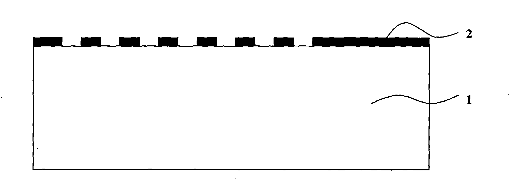
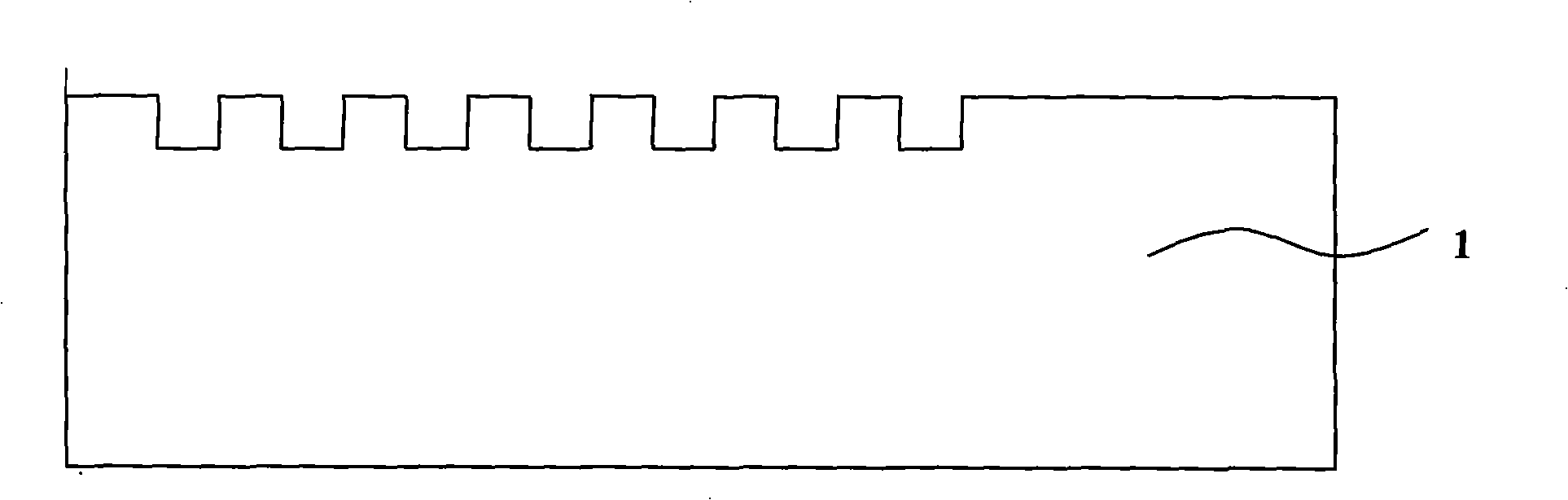
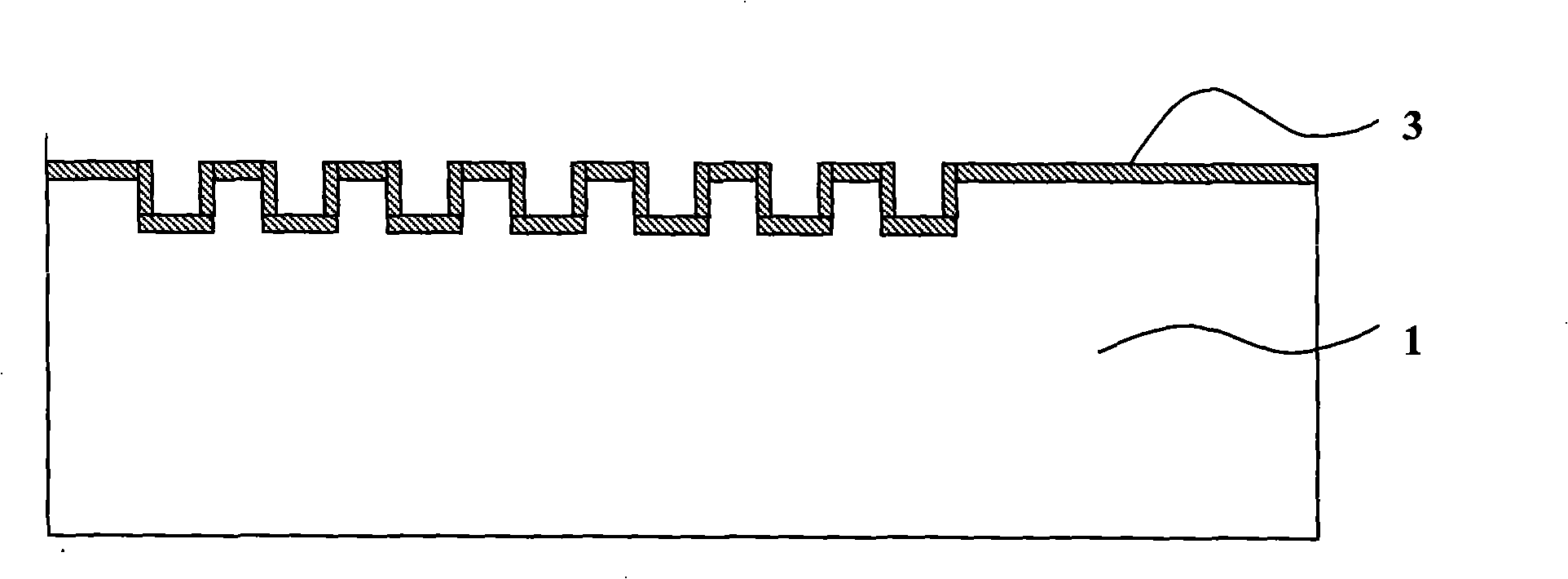
[0059] Refer to the attached Figure 1a Referring to Fig. 11, the present invention discloses a method for preparing SOI material of a double-sided dielectric tank, the steps are as follows:

[0060] a. Apply photoresist on the back of the top layer of silicon 1, and photoresist to form a photoresist mask 2, the photoresist mask 2 located below the source region and the channel region will continuously cover the back of the top layer of silicon 1, and the rest of the photoresist The mask 2 intermittently covers the back side of the top layer silicon 1, the back side of the top layer silicon 1 refers to the surface where the top layer silicon 1 is in contact with the dielectric buried layer, and the thickness of the photoresist mask 2 is 0.5-1.5 μm;

[0061] b. Remove the silicon not covered by the photoresist mask 2 on the back of the top layer of silicon 1 by dry etching to form a silicon groove with a depth of 200-2000nm, and then remove the mask;

[0062] c. A thin layer of...

Embodiment 2

[0073] A more preferred embodiment of the present invention is: on the basis of Example 1, in step d, SiO is deposited first and then densified. 2layer, the densification temperature is 850-1000°C, and the densification time is 0.5-2 hours.

Embodiment 3

[0075] On the basis of Example 1, another more preferred embodiment of the present invention is if required SiO 2 If the layer is thicker (>600nm), SiO is formed by densification after multiple depositions. 2 layer, the deposition temperature is still 700-900°C, each deposition is 200nm-600nm, the densification temperature is 850-1000°C, and the densification time is 0.5-2 hours.


PUM

PropertyMeasurementUnit
Thicknessaaaaaaaaaa

Abstract

The invention discloses a method for preparing double side dielectric groove part SOI material. Compared with the conventional bonding technology, before bonding, the method adds the following steps: 1. silicon groove etching on top layer silicon chip; 2. thermal growth and chemical vapor deposition of SiO2 layer; 3. removing the SiO2 layer positioned in a source area and under a channel region by etching; 4. deposition of polysilicon; 5. planarization of the polysilicon. As devices manufactured on the SOI material prepared by the method pass through reinforcing buried oxide layer electric field, the pressure resistance of the devices can be improved, and heat can be fully dispersed. Compared with devices with the conventional SOI structure, SOI devices prepared on the SOI material prepared by the method can utilize thinner top layer silicon and the buried oxide layer to reach the same pressure resistance, thus further reducing self-heating effect.

Description

technical field [0001] The invention proposes a method for preparing SOI material in a double-sided dielectric groove, which provides a substrate material for a power integrated circuit on the SOI material, especially a substrate material for a power device, and belongs to the technical field of semiconductor power devices and power integration. In particular, it relates to the technical field of material preparation of SOI power devices. Background technique [0002] SOI (Semiconductor On Insulator) technology has been widely concerned and applied because of its advantages of high speed, high integration, low power consumption, easy isolation, strong radiation resistance and no latch-up effect. The breakdown voltage of an SOI device is determined by the smaller of the lateral breakdown voltage and the vertical breakdown voltage. The lateral withstand voltage design of SOI high-voltage devices can follow the same junction termination technology and RESURF (REduced SURface F...

Claims


Application Information

Patent Timeline
IPC IPC(8): H01L21/762H01L21/20H01L21/3065H01L21/31
Inventor 罗小蓉雷磊傅达平高唤梅蒋辉雷天飞王元刚
Owner UNIV OF ELECTRONICS SCI & TECH OF CHINA
Why Eureka
Try Eureka