Pressure sensor based on Si-Si direct bonding and manufacturing method thereof

A pressure sensor and direct bonding technology, applied in chemical instruments and methods, fluid pressure measurement by changing ohmic resistance, manufacturing microstructure devices, etc., can solve problems such as device performance deterioration, achieve excellent performance, and avoid backside wet method Effects of corrosion and good airtight performance

Inactive Publication Date: 2009-10-07
江苏英特神斯科技有限公司
View PDF0 Cites 54 Cited by
  • Summary
  • Abstract
  • Description
  • Claims
  • Application Information

AI Technical Summary

Problems solved by technology

[0006] The present invention proposes a pressure sensor based on silicon-silicon direct bonding and its manufacturing method, which adopts silicon-silicon direct bonding technology to form a stress film and a sealed cavity, which not only avoids the long-term backside wet corrosion of conventional silicon pressure sensors, but also The size and residual stress of the stress film can be precisely contr

Method used


Image

  • Pressure sensor based on Si-Si direct bonding and manufacturing method thereof
  • Pressure sensor based on Si-Si direct bonding and manufacturing method thereof
  • Pressure sensor based on Si-Si direct bonding and manufacturing method thereof

Examples


Embodiment 1

[0033] Embodiment 1 relates to an absolute pressure sensor based on silicon-silicon direct bonding.

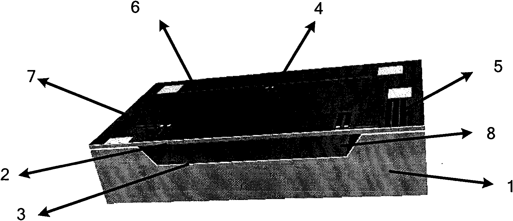
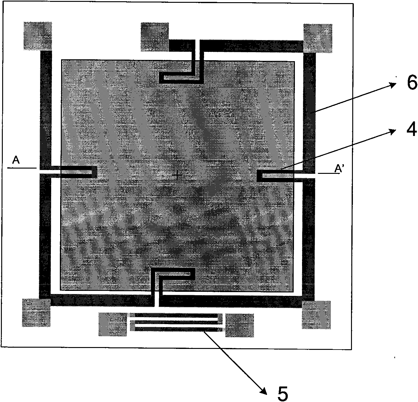
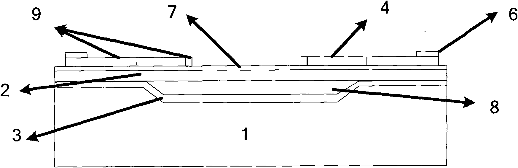
[0034] Such as figure 1 , figure 2 with image 3 As shown, a pressure sensor based on silicon-silicon direct bonding includes a silicon substrate 1 with a square shallow groove 8, on which is a single crystal silicon stress film 2, and between the silicon substrate 1 and the stress film 2 is a silicon dioxide The silicon layer 3; the square shallow groove 8 forms a sealed cavity with an inner vacuum during the direct bonding process of silicon and silicon. There are four P-type single crystal silicon piezoresistors 4 on the four sides of the stress film 2, and the four piezoresistors are etched from the same silicon chip. Between the stress film 2 and the piezoresistor 4 is a silicon dioxide layer 7; the piezoresistive turning section and the lead area are formed of low-resistance connection and ohmic contact with boron-doped silicon 9, and the gold lead 6 is used to form ...

Embodiment 2

[0037] Embodiment 2 Prepare an absolute pressure sensor according to the method of the present invention, and the specific process flow is as follows Figure 4 shown, including the following steps:

[0038] 1. Substrate Preparation

[0039] a) Choose a 6-inch N-type silicon wafer A with a crystal orientation, and perform thermal oxidation, SiO 2 The thickness is 500nm.

[0040] b) performing the first photolithography to define a square stress film pattern. Using an anisotropic etching solution, such as 25% TMAH etching solution, etching is carried out at 85° C. for 30 minutes to form a square shallow groove. Remove the silicon dioxide on the surface of silicon wafer A, and re-grow SiO with a thickness of 500nm by thermal oxidation 2 .

[0041] 2. Preparation of SOI wafers by silicon-silicon bonding for the first time

[0042] a) Simultaneously perform RCA surface activation cleaning on silicon wafer B and silicon wafer C, rinse with deionized water, and then perform dr...

Embodiment 3

[0051] Embodiment 3 Prepare a relative pressure sensor according to the method of the present invention, and the specific process flow includes the following steps:

[0052] 1. Substrate Preparation

[0053] a) Choose a 6-inch N-type silicon wafer A with a crystal orientation, and perform thermal oxidation, SiO 2 The thickness is 500nm.

[0054] b) performing the first photolithography to define a square stress film pattern. Using an anisotropic etchant, such as a 25% TMAH etchant, etch at 85° C. until the corrosion stops at the 111 crystal plane. Use a VG202MKII special thinning machine to mechanically grind the bonding sheet until the through-silicon holes are exposed (at this time, the thickness of the silicon layer is about 400 μm).

[0055] 2. Preparation of SOI wafers by silicon-silicon bonding for the first time

[0056] a) Simultaneously perform RCA surface activation cleaning on silicon wafer B and silicon wafer C, rinse with deionized water, and then perform dry...


PUM

PropertyMeasurementUnit
Thicknessaaaaaaaaaa

Abstract

The invention discloses a pressure sensor based on Si-Si direct bonding, comprising a silicon substrate (1) with a shallow groove (8); the silicon substrate (1) is provided with a single crystal silicon stress membrane (2); a silicon dioxide layer (3) is arranged between the silicon substrate (1) and the stress membrane (2); four P-type single crystal silicon piezoresistors (4) are arranged on the stress membrane (2); an insulating medium silicon dioxide layer (7) is arranged among the stress membrane (2) and the piezoresistors (4); and a Wheatstone bridge is formed among the piezoresistors (4) by utilizing concentrated boron doped silicon (9) and a golden lead (6). The pressure sensor adopts Si-Si direct bonding technology to form the stress membrane and the sealing cavity; the piezoresistors thereof adopt silicon dioxide as an insulating layer and the working temperature can be up to 300 DEG C; and the pressure sensor has firm structure and excellent performance and can meet the requirements on high-temperature pressure sensors in the fields of automobile, aerospace and the like. The invention also relates to a manufacturing method of the pressure sensor.

Description

technical field [0001] The invention relates to a pressure sensor based on MEMS (micro-electro-mechanical system) technology and a manufacturing method thereof, in particular to a pressure sensor based on silicon-silicon direct bonding and a manufacturing process thereof. Background technique [0002] Silicon pressure sensor is an outstanding representative of the great success of micromachining technology, and has a wide range of applications in many fields such as automotive systems, industrial control, environmental monitoring and measurement, and biomedical diagnosis. The piezoresistive silicon pressure sensor is the earliest realized type of pressure sensor, and its working principle is the piezoresistive effect first discovered by C.S.Smith in 1954. The piezoresistive coefficient of semiconductor materials, especially P-type doped single crystal silicon, is several orders of magnitude larger than that of metals. [0003] The structure of a typical piezoresistive press...

Claims


Application Information

Patent Timeline
IPC IPC(8): G01L1/18G01L1/20G01L9/06B81B7/02B81C5/00B81C1/00B81C99/00
Inventor 沈广平何野徐波
Owner 江苏英特神斯科技有限公司
Why Eureka
Try Eureka