Semiconductor packaging base plate and manufacturing method thereof

A technology for encapsulating substrates and semiconductors, which is applied in semiconductor/solid-state device manufacturing, semiconductor devices, semiconductor/solid-state device components, etc. Effects of thickness, avoidance of stress concentration, and optimum bonding strength

Active Publication Date: 2009-10-28
UNIMICRON TECH CORP
View PDF0 Cites 11 Cited by
  • Summary
  • Abstract
  • Description
  • Claims
  • Application Information

AI Technical Summary

Problems solved by technology

[0009] However, in the above-mentioned existing manufacturing method, the size of the opening 120 of the insulating protection layer and the size of the opening 140 of the resistance layer are very fine, generally about 50 μm-60 μm, so alignment is extremely difficult. In order to make the opening of the resistance layer 140 can be aligned with the opening 120 of the insulating protective layer. Usually, the size of the opening 140 of the resistive layer is increased to reduce the difficulty of alignment and improve the alignment accuracy of the process. When the opening 120 of the insulating protective layer has a diameter of When it is smaller, the size of the resistive layer opening 140 may also be increased to twice the size of the insulating protective layer opening 120 due to the limitation of machine precision.
[0010] However, enlarging the size of the resistive layer opening 140 will result in the formation of side edges 151 on the top surface of the conductive pillars 15, so that the distance between the conductive pillars 15 must be increased. Fine-pitch pre-solder bumps formed on
[0011] And the side edge 151 of the conductive pillar 15 is protruding from the surface of the insulating protection layer 12, and it is easy to generate stress due to temperature change and CTE (coefficient of thermal expansion) difference, and it is concentrated between the conductive pillar 15 and the side edge 151, and In case of damage

Method used


Image

  • Semiconductor packaging base plate and manufacturing method thereof
  • Semiconductor packaging base plate and manufacturing method thereof
  • Semiconductor packaging base plate and manufacturing method thereof

Examples


no. 1 example

[0044] see Figure 2A to Figure 2J , are the semiconductor package substrate and the manufacturing method thereof of the present invention.

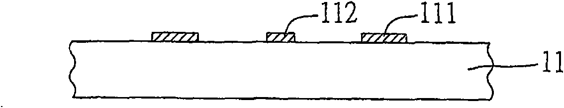
[0045] see Figure 2A Firstly, a substrate body 20 with a dielectric layer 21 formed on at least one surface is provided, and a conductive layer 22 is formed on the dielectric layer 21, and the conductive layer 22 is mainly used as a current conduction path required for electroplating metal materials described later, which It can be composed of metal or deposited several layers of metal layers, such as single-layer or multi-layer structures selected from copper, tin, nickel, chromium, titanium, copper-chromium, etc., or can use polyacetylene, polyaniline or organic sulfur polymers, etc. Conductive polymer materials.

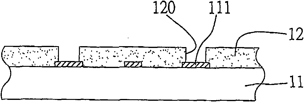
[0046] see Figure 2B A first resist layer 23 is formed on the conductive layer 22 by means of printing, spin coating or bonding, and a plurality of openings 230 are formed on the first resist layer 23 through patterning p...

no. 2 example

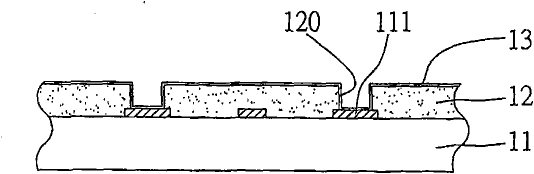
[0061] see Figure 3A and Figure 3B , is another implementation method of the present invention, which is different from the previous embodiment in that the opaque area of ​​the photomask completely covers each of the conductive pillars and includes the regions between the conductive pillars.

[0062] Such as Figure 3A As shown, it is a continuation of the first embodiment Figure 2I The opaque region 281' of the photomask 28 completely covers each of the conductive pillars 26 and the area between each of the conductive pillars 26, so that the insulating protection layer 27 not covered by the opaque region 281 exposure.

[0063] see Figure 3B , and then remove the surface of the insulating protection layer 27 that has not been exposed, and then form an exposed portion that is a recessed region 272 on the surface of the insulating protection layer 27. The recessed region 272 does not penetrate through the insulating protection layer 27 and exposes each of the The top su...


PUM


Abstract

The invention relates to a semiconductor packaging base plate and a manufacturing method thereof. The semiconductor packaging base plate comprises a base plate body, a plurality of conductive poles and an insulating protection layer, wherein at least one surface of the base plate body is provided with a plurality of electrical connection gaskets; the conductive poles respectively completely wrap each electrical connection gasket; and the insulating protection layer is formed on the surface of the base plate body and is provided with an exposure part for exposing the conductive poles, thus the invention can shorten the distances among the conductive poles, can prevent the stress from being concentrated and the bottom filling materials from overflowing and can also lower the packaging height.

Description

technical field [0001] The invention relates to a semiconductor packaging substrate and a manufacturing method thereof, in particular to a semiconductor packaging substrate formed with conductive columns and a manufacturing method thereof. Background technique [0002] In the current Flip Chip technology, there are electrode pads on the active surface of the semiconductor chip of the integrated circuit (IC), and the organic circuit board also has electrical connection pads corresponding to the electrode pads. A solder structure or other conductive adhesive material is formed between the pad and the electrical connection pad of the circuit board, and the solder structure or conductive adhesive material provides the electrical connection and mechanical connection between the semiconductor chip and the circuit board, and the related manufacturing process that is, Figure 1A to Figure 1F shown. [0003] see Figure 1A Firstly, a circuit board 11 with a plurality of electrical ...

Claims


Application Information

Patent Timeline
Patent Type & Authority Applications(China)
IPC IPC(8): H01L23/498H01L21/48
CPCH01L2924/0002
Inventor 胡文宏
Owner UNIMICRON TECH CORP
Why Eureka
Try Eureka