Monolithic integrated non-refrigerated infrared/ultraviolet double-color detector and manufacture method thereof
An uncooled infrared and two-color detector technology, which is applied in the field of photoelectric detectors, can solve the problems of bulky refrigeration systems and the difficulty of realizing low-cost portable system requirements, so as to reduce the size of devices, improve the probability of detection and identification, and reduce processing costs. cost effect
- Summary
- Abstract
- Description
- Claims
- Application Information
AI Technical Summary
Problems solved by technology
Method used
Image
Examples
Embodiment 1
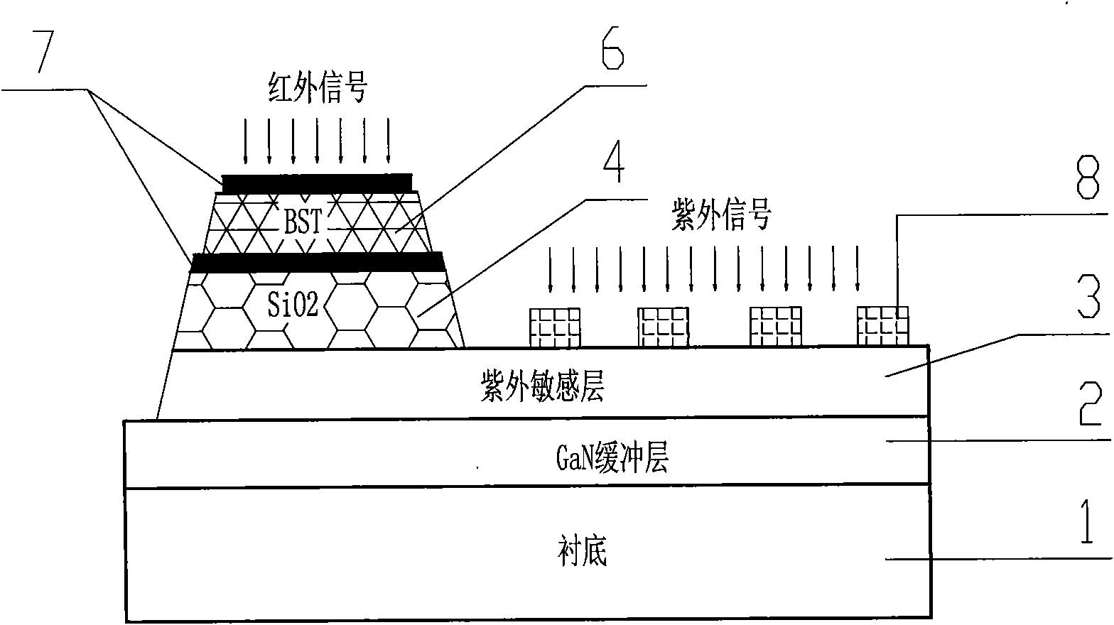
[0020] This embodiment is a specific manufacturing process of a BST / GaN uncooled monolithic integrated infrared / ultraviolet dual-color detector. The infrared / ultraviolet dual-color detector manufactured by using this method and material has the following characteristics: figure 2 For the structure shown, the specific steps are as follows:
[0021] 1) Firstly, the basic material structure is grown, and a 1.5μm GaN buffer layer and a 2μm non-doped GaN ultraviolet absorption layer (Si doping concentration is 1×10) are grown on a sapphire substrate with MOCVD system. 16 cm-3); 2μm porous silica grown by gel sol method and 200nm SiNx grown by PECVD as isolation layer; Pt / Ti deposited by magnetron sputtering system, 30nm Pt / 100nm Ti composite metal film as infrared detection Bottom electrode of the detector; use a magnetron sputtering system to deposit barium strontium titanate (BST) film with a thickness of 500nm and a temperature of 700℃; then use conventional semiconductor photolith...
Embodiment 2
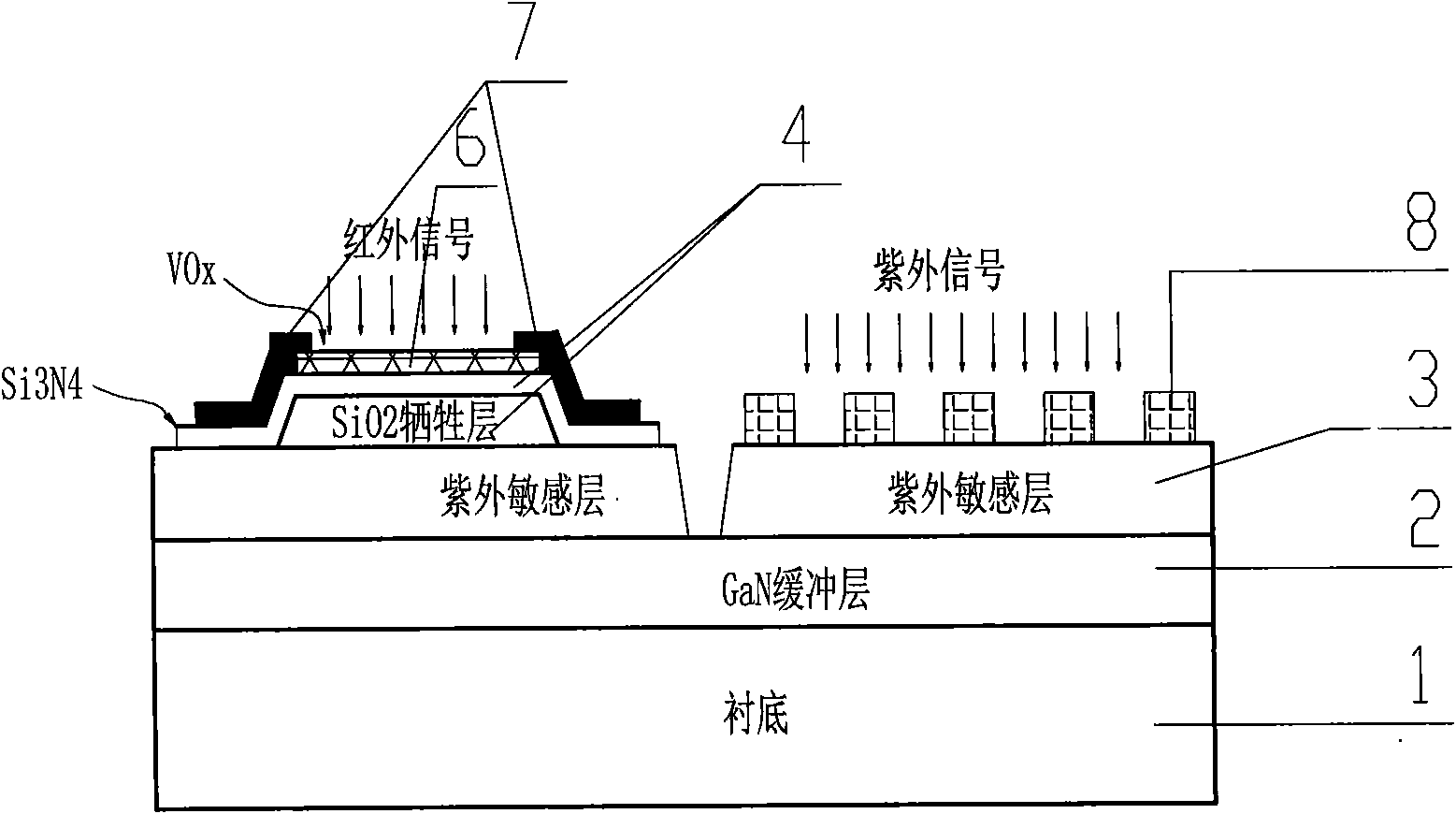
[0031] This embodiment is a specific manufacturing process of a VOx / GaN uncooled monolithic integrated infrared / ultraviolet dual-color detector. The infrared / ultraviolet dual-color detector manufactured by using this method and materials has the following characteristics: image 3 For the structure shown, the specific steps are as follows:
[0032] 1) On a sapphire substrate, a 1.5μm GaN buffer layer and a 2μm non-doped GaN ultraviolet absorption layer (Si doping concentration is 1×10 16 cm-3), such as Figure 5a Shown
[0033] 2) Use PECVD to grow 2.5μm thick porous structure SiO2 as the sacrificial layer, such as Figure 5b Shown
[0034] 3) Photoetch the support leg pattern of the bridge deck, and remove the SiO2 at the support leg position by reactive ion etching, such as Figure 5c Shown
[0035] 4) PECVD growth of 0.5μm Si3N5 bridge support layer, such as Figure 5d Shown
[0036] 5) Use magnetron sputtering to grow 50nm VOx film; use photoresist to mask and etch sensitive el...
PUM
 Abstract
Description
Claims
Application Information


