Power type LED lamp, encapsulation process and reflow soldering process equipment thereof

A LED lamp and reflow soldering technology, which is applied in welding equipment, metal processing equipment, lighting and heating equipment, etc., can solve the problems of high thermal resistance of the connection interface, poor high temperature aging resistance, etc. The effect of poor high temperature aging properties

Inactive Publication Date: 2012-07-25
TIANJIN UNIV
View PDF1 Cites 0 Cited by
  • Summary
  • Abstract
  • Description
  • Claims
  • Application Information

AI Technical Summary

Problems solved by technology

It can effectively solve the problems of high thermal resistance at the connection interface and poor high temperature aging resistance in the package of power LED lamps

Method used


Image

  • Power type LED lamp, encapsulation process and reflow soldering process equipment thereof
  • Power type LED lamp, encapsulation process and reflow soldering process equipment thereof
  • Power type LED lamp, encapsulation process and reflow soldering process equipment thereof

Examples


Embodiment 1

[0039] 1) if Figure 5 As shown, use a quantitative dispensing machine or a screen printing machine to apply lead-free solder paste 6 on the position where the heat sink needs to be installed on the heat sink seat 3, and then place the chip-heat sink body packaged by low-temperature sintering on the solder paste and apply some pressure to evenly distribute the solder paste between the heat sink and heat sink.

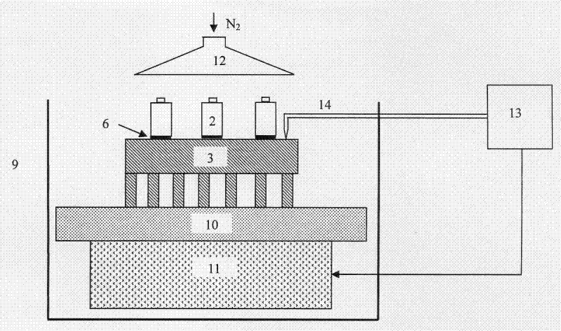
[0040] 2) Put the whole sample into image 3 Reflow soldering is performed in the dedicated reflow oven shown. The equipment is composed of furnace body jacket 9, hot plate 10, resistance heater 11, cooler cover 12, temperature controller 13 and thermocouple 14 and other parts. The lead-free solder paste 6 is pre-coated between the radiator seat 3 and the chip-heat sink body 2 and then placed on the hot plate 10; the thermocouple 14 is fixed on the upper surface of the radiator seat to monitor the temperature of the workpiece surface in real time . The temperature c...

Embodiment 2

[0044] Embodiment 2: as Figure 4-6 shown.

[0045] First level packaging process:

[0046] 1) if Figure 4 As shown, the prepared nano-silver paste 5 is quantitatively injected on the upper surface of the heat sink 2 by a dispenser, and then the LED chip 1 is placed on the metal paste with vacuum tweezers and pressed tightly, so that the nano-metal paste is placed between the chip and the metal paste. Spread evenly between heat sinks, and control the thickness of the paste layer within the range of 10-40um.

[0047] 2) Put the pre-prepared chip-heat sink body of the nano-metal paste into a vacuum desiccator for 24 hours, so that the organic solvent in the metal paste can be slowly and completely evaporated, and at the same time it will not be in the adhesive layer. The formation of pores affects the quality of subsequent sintering.

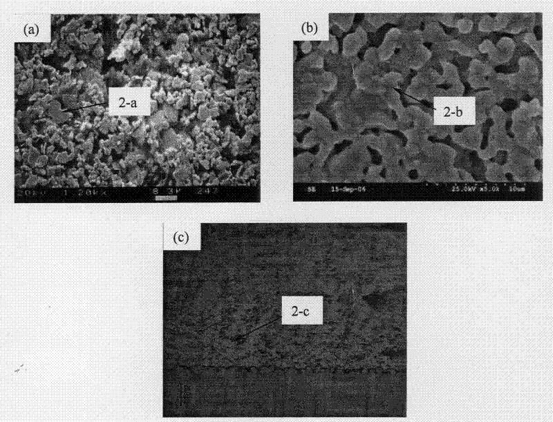
[0048] 3) Put the fully dried chip-heat sink body 2 into a sintering furnace for low-temperature sintering. The specific sintering paramete...

Embodiment 3

[0054] Embodiment 3: as Figure 7 shown.

[0055] 1) The low-temperature sintering process of the chip-heat sink is the same as in Embodiment 1, except for the secondary packaging. Such as Figure 7 As shown, the boss 3-1 required for welding the heat sink is prefabricated on the radiator seat, and the height of the boss is consistent with the thickness of the hollow PCB board to be pasted later. After pasting the hollow PCB circuit board, the upper surface of the boss is on the same plane as the pad on the PCB, and a lead-free solder paste layer is printed on the boss and the corresponding PCB pad with a screen printing machine6 .

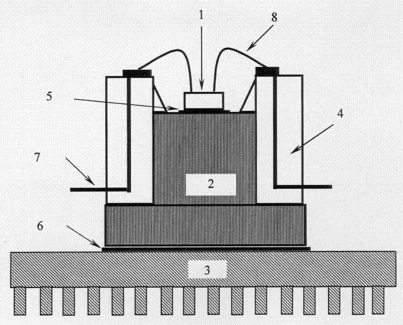
[0056]2) Install the reflective cup 4 with the external electrode lead 7 on the chip-heat sink body 2 after the first-level packaging, and then use the gold wire 8 to interconnect with the chip electrode through a wire bonding process.

[0057] 3) Mount the chip-heat sink body with the reflective cup installed on the heat sink seat 3 pre-coate...


PUM

PropertyMeasurementUnit
melting pointaaaaaaaaaa

Abstract

The invention relates to a power type LED lamp, an encapsulation process and reflow soldering process equipment thereof. In the power type LED lamp, two bonding interfaces with metallurgy connection are connected among an LED chip, heat sink and a radiator to establish a complete metal radiation channel with low thermal resistance for heat generated in a luminescence process of the LED chip. The chip and the heat sink are connected by adopting nanometer metal powder low temperature sintering technology; the heat sink and a radiator seat are connected by adopting lead-free reflow soldering process. The lead-free reflow soldering is a reflow soldering process of heating from one side of the bottom surface of the radiator seat and heating a single side of the bottom surface blowing cooling gas from one side of the upper chip-heat sink body. The maximum operation temperature and the heat conductivity of a connection interface layer of a nanometer silver paste sintering process and the lead-free reflow soldering process are significantly superior to those of the prior applied conductive adhering process either, and are also superior to those of a tin-lead reflow soldering process. Organic combination of the two processes are applied to manufacture of the power type LED so as to greatly improve the radiation performance and high temperature resistance of the LED.

Description

technical field [0001] The invention belongs to the technical field of electronic manufacturing, and relates to a power type LED lamp with the feature of all-metal connection and its packaging process and reflow soldering process equipment. Background technique [0002] With the breakthrough of the third-generation semiconductor material gallium nitride and the advent of blue, green, and white light-emitting diodes, following the microelectronics revolution triggered by semiconductor technology, a new industrial revolution-the lighting revolution is being bred, and its symbol is the semiconductor Lamps will gradually replace incandescent and fluorescent lamps. Semiconductor lamps use light-emitting diodes (LEDs) as new light sources. Under the same brightness, the power consumption is only 1 / 10 of that of ordinary incandescent lamps, but the life span can be extended by 100 times. Therefore, semiconductor lighting (also known as solid-state lighting) has energy-saving and lo...

Claims


Application Information

Patent Timeline
Patent Type & Authority Patents(China)
IPC IPC(8): F21V29/00F21V19/00H01L23/36H01L33/00B23K1/008F21Y101/02F21V29/70F21V29/90F21Y115/10
CPCH01L2224/48091H01L2224/48227H01L2224/73265
Inventor 程方杰陈旭陆国权
Owner TIANJIN UNIV
Why Eureka
Try Eureka