Preparation method of low thermal resistance thermal interface

A technology of thermal interface and low thermal resistance, which is applied in chemical instruments and methods, heat exchange materials, semiconductor/solid-state device manufacturing, etc., can solve the problems of not very obvious effect and high thermal resistance of interface contact, and achieve strong implementability, The effect of reducing the contact thermal resistance of the interface and increasing the contact probability

Inactive Publication Date: 2009-12-23
HUAZHONG UNIV OF SCI & TECH
View PDF0 Cites 16 Cited by
  • Summary
  • Abstract
  • Description
  • Claims
  • Application Information

AI Technical Summary

Problems solved by technology

Studies have shown that less than 1% of CNTs are interconnected up and down, and the remaining large number of CNTs do not touch the target substrate at all, resulting in high interface contact thermal resistance.
Although some improvement measures have been proposed in recent years, including the use of metal interlayer technology (such as Figure 5 , 12 is the VACNT growth substrate, 18

Method used


Image

  • Preparation method of low thermal resistance thermal interface
  • Preparation method of low thermal resistance thermal interface
  • Preparation method of low thermal resistance thermal interface

Examples


Embodiment 1

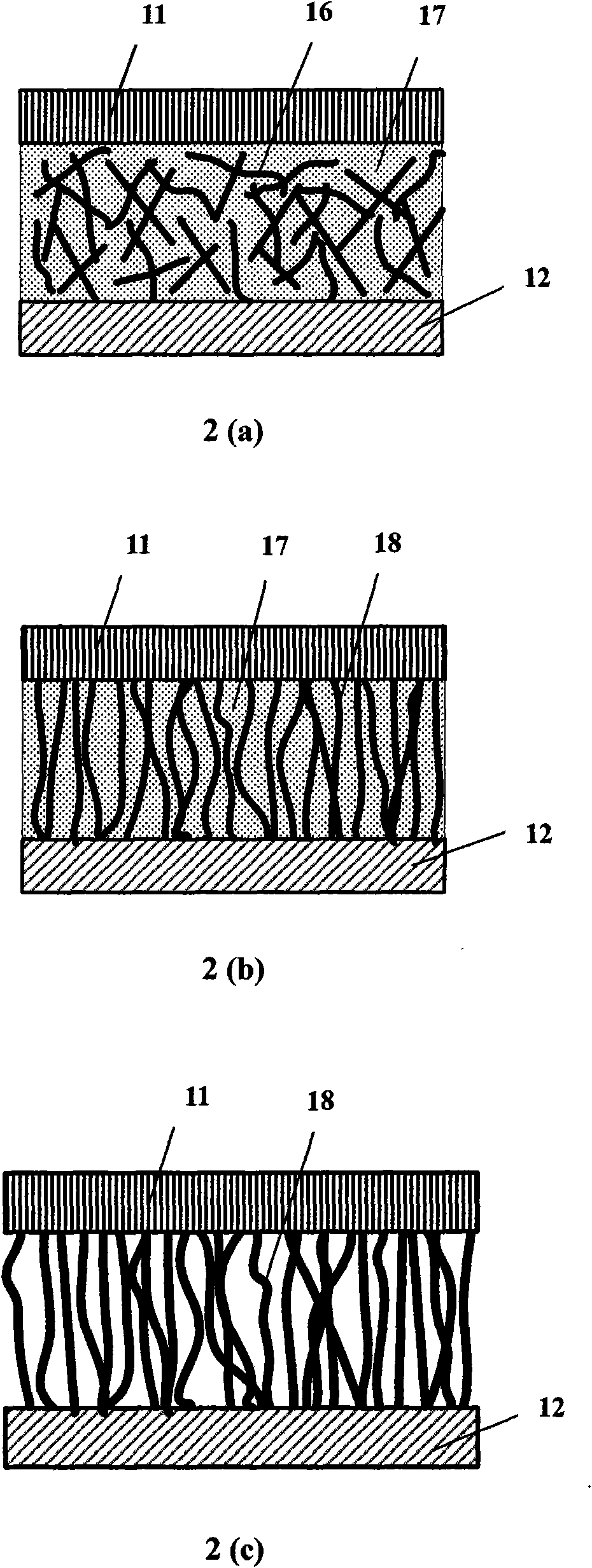
[0024] 1. Catalyst deposition: adopt atomic layer deposition (ALD) technology to deposit 10 nanometer thick Ni or Fe layer on copper substrate 21, as the catalyst layer 22 of CNT growth;

[0025] 2. Catalyst cracking: using a high temperature annealing process at a temperature of 650°C to crack the catalyst layer 22 into catalyst particles 23;

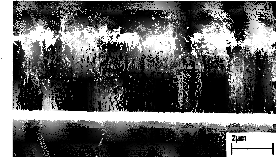
[0026] 3. Growth of carbon nanotubes: using chemical vapor deposition (CVD) technology to prepare oriented growth carbon nanotubes (VACNT) 18 on the copper substrate 21, with a diameter of about 20 nanometers and a thickness of about 20 microns;

[0027] 4. VACNT modification: using water vapor etching technology to remove the catalyst particles 23 remaining on the top of VACNT 18, and at the same time reduce the winding of the top of VACNT;

[0028] 5. Deposition of magnetic material layer: deposition techniques include evaporation, sputtering, atomic layer deposition (ALD) and other thin film deposition techniques. The magnetic mater...

Embodiment 2

[0035] 1. The copper substrate 21 for growing carbon nanotubes is replaced with a silicon substrate 33, and other VACNT magnetization processes are the same as in Embodiment 1, including catalyst deposition and cracking, carbon nanotube growth and modification, magnetic material layer deposition and heat treatment;

[0036] 2. Electromagnetic alignment: see Figure 9 Place the silicon substrate 33 grown with VACNT18 in the middle of the induction coil 34, turn on the high-frequency power supply 35, and under the action of the electromagnetic field 36, the magnetic particles 26 at the top of the VACNT 18 are subjected to magnetic force, so that the VACNT 18 are parallel to each other;

[0037] 3. Solder bonding: After depositing metal titanium and tin layer 38 (wherein the thickness of the titanium layer is 20 nanometers, and the thickness of the tin layer is 5 microns) on the lower surface of the gallium nitride (GaN) substrate 37, it is placed on a substrate grown with VACNT24...


PUM

PropertyMeasurementUnit
Diameteraaaaaaaaaa
Thicknessaaaaaaaaaa
Thicknessaaaaaaaaaa

Abstract

The invention provides a preparation method of low thermal resistance thermal interface. Firstly a vertically aligned carbon nano tube (VACNT) is prepared on a substrate, then the VACNT is modified and magnetized, and then contact probability between the VACNT and a target substrate is improved by magnetic aiming, and finally bonding between the VACNT and the target substrate is realized by bonding technology. Owing to the combined action of magnetic force and pressure, conformal contact is formed between the VACNT and the target substrate, thus effectively reducing interface contact thermal resistance. The invention solves the difficult problem that the VACNT is directly used as thermal interface material, provides a new way for research and development of nano encapsulation and interconnection and low thermal resistance encapsulation technology, and promotes the research of optoelectronic integration technology and the research and development of power devices.

Description

technical field [0001] The invention relates to the technical field of low thermal resistance packaging, in particular to a method for preparing a low thermal resistance thermal interface using oriented growth carbon nanotubes directly as a thermal interface material. Background technique [0002] Semiconductor technology has been developing along the direction of miniaturization and integration. Take a computer CPU chip as an example. At present, the number of transistors in a single chip has exceeded 1 billion, while the size of its interconnection lines is only tens of nanometers. The ultra-miniaturization and high integration of electronic components pose new challenges to the thermal performance of the system: on the one hand, miniaturization makes the overall size of the device smaller and smaller, and the processing feature size is also continuously reduced. The high heat flux generated by micro-nano devices and systems during motion can easily lead to poor heat diss...

Claims


Application Information

Patent Timeline
IPC IPC(8): H01L21/48H01L23/373C09K5/14
CPCH01L2924/0002
Inventor 陈明祥刘胜
Owner HUAZHONG UNIV OF SCI & TECH
Why Eureka
Try Eureka