Polymer/inorganic nano-crystal hybrid solar cell and manufacture method thereof
A technology of solar cells and inorganic nanometers, applied in the direction of photosensitive equipment, etc., can solve the problems of low energy conversion efficiency of batteries, and achieve the effects of improving energy conversion efficiency, increasing open circuit voltage, and increasing short circuit current
- Summary
- Abstract
- Description
- Claims
- Application Information
AI Technical Summary
Problems solved by technology
Method used
Image
Examples
Embodiment 1
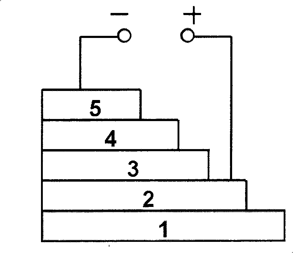
[0031] In an inert atmosphere glove box, MEH-PPV and ZnO were dissolved in chlorobenzene:methanol with a volume ratio of 95:5 in a mixed solvent with a mass ratio of 1:3.3 to obtain a mixed solution, and the mixed solution was magnetically stirred for 12 hours; The concentration of MEH-PPV described above is 3.5 mg per milliliter; the particle diameter of ZnO is 5 nanometers, and the concentration of ZnO is 11.55 mg per milliliter;
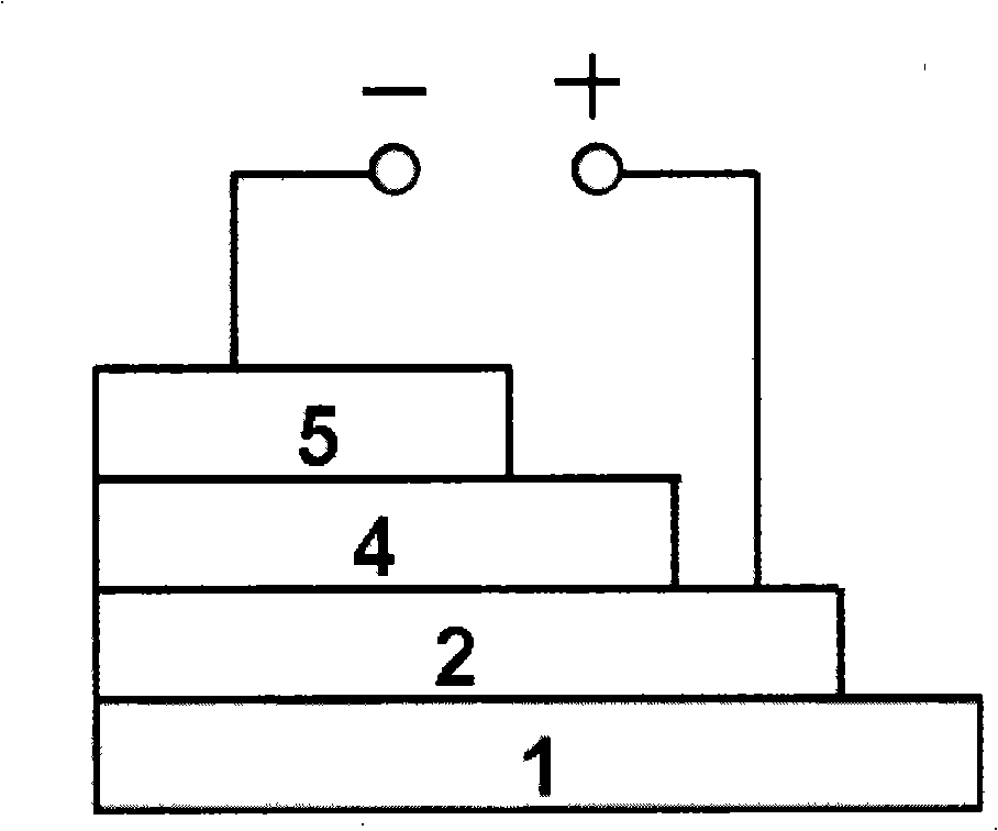
[0032] Etching the indium tin oxide anode layer 2 with a thickness of 120 nm on the glass substrate 1 into thin strips with a width of 4 mm, cleaning the etched thin strips of ITO glass, putting them in an oven, drying them at 120 ° C, and then Place the workpiece on the carriage of the coating machine, pass through the filter head of 0.45 micron, and Cu 2 The dispersion of O is evenly coated on the whole sheet, and is spin-coated to form a film at a speed of 450 revolutions per minute, and a layer of Cu with a thickness of 80 nanometers is formed...
Embodiment 2
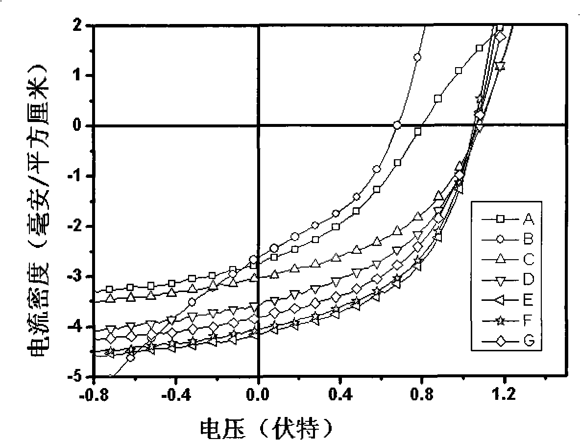
[0036] The device structure and preparation method are the same as in Example 1, except that Cu 2 O spin-coating at 1000 rpm to obtain Cu with a thickness of 50 nm 2 O hole collection layer. The device structure is ITO(120nm) / Cu 2 O(50nm) / MEH-PPV:ZnO(140nm) / Al(80nm).
Embodiment 3
[0038] The device structure and preparation method are the same as in Example 1, except that Cu 2 O spin-coated at 2000 rpm to obtain Cu with a thickness of 40 nm 2 O hole collection layer. The device structure is ITO(120nm) / Cu 2 O(40nm) / MEH-PPV:ZnO(140nm) / Al(80nm).
PUM
| Property | Measurement | Unit |
|---|---|---|
| Thickness | aaaaa | aaaaa |
| Thickness | aaaaa | aaaaa |
| Thickness | aaaaa | aaaaa |
Abstract
Description
Claims
Application Information


