
Solar cell device and method for manufacturing same

A technology for solar cells and devices, applied in the fields of electric solid state devices, semiconductor/solid state device manufacturing, electrical components, etc., can solve problems such as low energy conversion efficiency of solar cells

Inactive Publication Date: 2014-12-31
OCEANS KING LIGHTING SCI&TECH CO LTD +2
View PDF6 Cites 0 Cited by
  • Summary
  • Abstract
  • Description
  • Claims
  • Application Information

AI Technical Summary

Problems solved by technology

Currently, conventional solar cells have low energy conversion efficiencies

Method used


Image

  • Solar cell device and method for manufacturing same
  • Solar cell device and method for manufacturing same
  • Solar cell device and method for manufacturing same

Examples


preparation example Construction

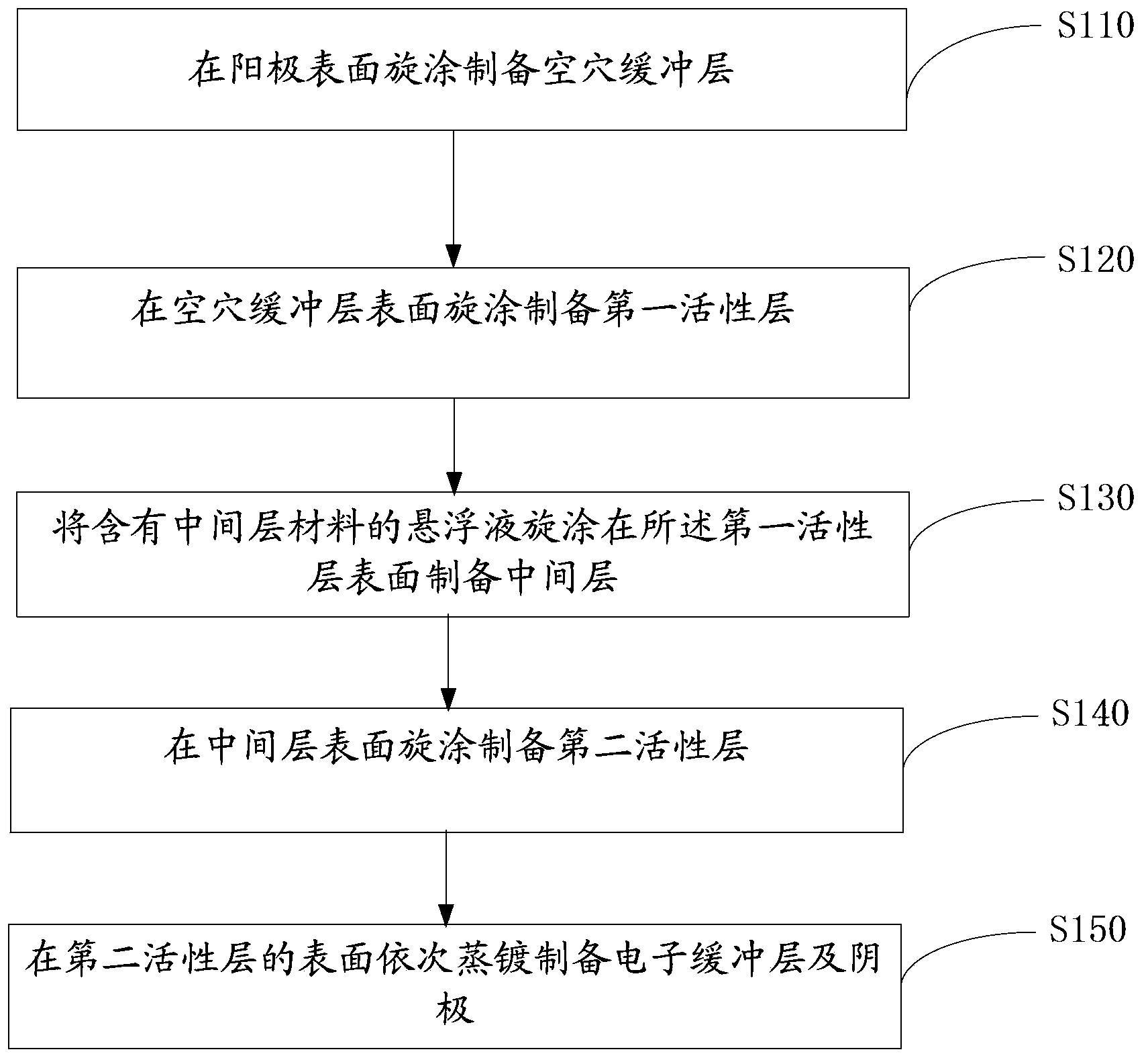
[0034] Please also see figure 2 , the preparation method of the solar cell device 100 of an embodiment, it comprises the following steps:

[0035] Step S110 , preparing a hole buffer layer 20 on the surface of the anode 10 by spin coating.

[0036] The anode 10 is indium tin oxide glass (ITO), fluorine doped tin oxide glass (FTO), aluminum doped zinc oxide glass (AZO) or indium doped zinc oxide glass (IZO).

[0037] In this embodiment, the pretreatment of the anode 10 includes removing organic pollutants on the surface of the anode 10 and performing oxygen ion treatment on the anode 10 . The anode 10 is ultrasonically cleaned with detergent, deionized water, acetone, ethanol, and isopropanone for 15 minutes to remove organic pollutants on the surface of the substrate 10; the anode 10 is treated with oxygen ion for 5 minutes to 15 minutes, and the power is 10 minutes. ~50W.

[0038] The hole buffer layer 20 is prepared by spin-coating a solution containing a hole buffer mater...

Embodiment 1

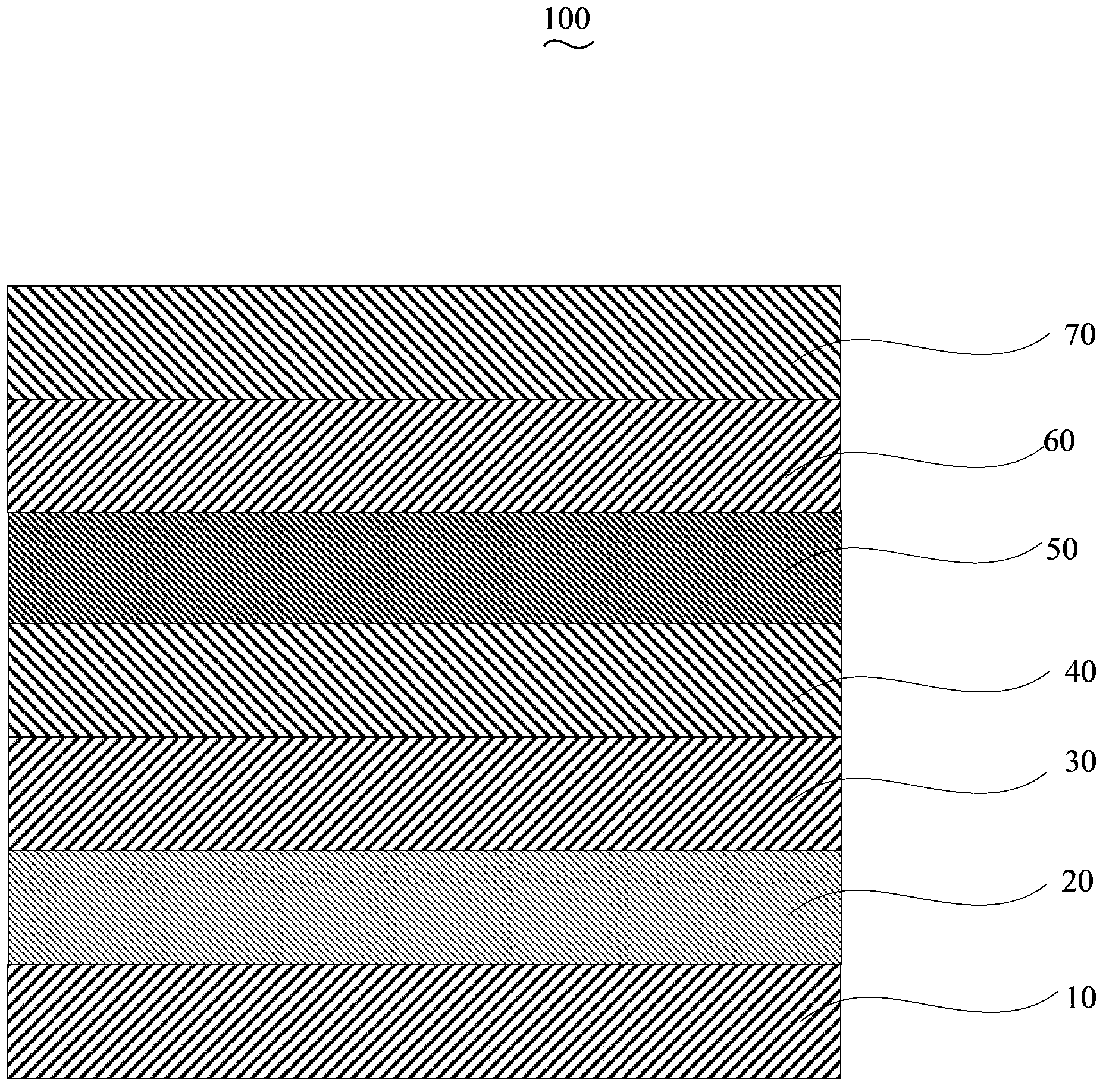
[0054] The structure prepared in this embodiment is: ITO / PEDOT:PSS / P3HT:PC 61 BM / Bphen:FeCl 3 :CuPc / P3HT:PC 61 BM / LiF / Al solar cell devices. Wherein, " / " indicates a stacked structure, and ":" indicates doping or mixing, and the following embodiments are the same.

[0055] First, carry out photolithography treatment on ITO, cut it into the required size, and then use detergent, deionized water, acetone, ethanol, and isopropanol to sonicate for 15 minutes each to remove organic pollutants on the glass surface; clean the conductive substrate Oxygen plasma treatment was carried out, the treatment time was 10min, and the power was 20W; the hole buffer layer was prepared by spin coating, the material was PEDOT:PSS with a mass ratio of 2:1, the mass fraction of PEDOT was 2%, and the spin coating speed was 4000rpm. The time is 15s, after spin-coating, heat at 200°C for 30min, and the thickness is 70nm; spin-coat the first active layer, the first active layer is composed of P3HT an...

Embodiment 2

[0062] The structure prepared in this example is IZO / PEDOT:PSS / P3HT:PC 61 BM / TAZ:FeBr 3 :MgPc / P3HT:PC 61 BM / Cs 2 CO 3 / Au solar cell devices.

[0063] First, IZO is subjected to photolithography treatment, cut into the required size, and then ultrasonicated with detergent, deionized water, acetone, ethanol, and isopropanol for 15 minutes each to remove organic pollutants on the glass surface; after cleaning, clean the conductive substrate Oxygen plasma treatment was carried out, the treatment time was 15min, and the power was 10W; the hole buffer layer was prepared by spin coating, the material was PEDOT:PSS with a mass ratio of 2:1, the mass fraction of PEDOT was 5%, and the spin coating speed was 6000rpm. The time is 30s, after spin-coating, heat at 100°C for 60min, the thickness is 20nm; spin-coat the first active layer, the first active layer is composed of P3HT and PC with a concentration of 8mg / ml 61 The solution of BM was spin-coated, the solvent was toluene, P3HT ...


PUM


Abstract

The invention discloses a solar cell device. The solar cell device comprises an anode, a hole buffer layer, a first active layer, an intermediate layer, a second active layer, an electron buffer layer and a cathode which are sequentially stacked on one another. The first active layer and the second active layer are made of mixtures of poly-3-hexyl-thiophene and 6,6-phenyl-C<61>-methyl butyrate, the intermediate layer is made of ferric salt, phthalocyanine compounds and electron transport materials, the selected ferric salt comprises at least one type of ferric chloride, ferric tribromide and ferric sulfid, the selected phthalocyanine compounds comprise at least one type of copper phthalocyanine, zinc phthalocyanine, magnesium phthalocyanine and vanadium phthalocyanine, and the selected electron transport materials comprise at least one type of 4,7-diphenyl-1,10-phenanthroline, 3-(biphenyl-4-based)-5-(4-tertiary butyl phenyl)-4-phenyl-4H-1,2,4-triazole and N-aryl benzimidazole. The solar cell device has the advantage of high energy conversion efficiency. The invention further provides a method for manufacturing the solar cell device.

Description

technical field [0001] The invention relates to a solar battery device and a preparation method thereof. Background technique [0002] Solar cell devices have been widely used due to their advantages of cheapness, cleanliness, and renewability. The currently commonly used solar cell device structure includes an anode, a hole buffer layer, a first active layer, an electron buffer layer and a cathode stacked in sequence. After the excitons in the first active layer are separated to generate holes and electrons, the holes reach the anode, and the electrons reach the cathode, where they are collected by the electrodes to form effective energy conversion. Currently, conventional solar cells have low energy conversion efficiencies. Contents of the invention [0003] Based on this, it is necessary to provide a solar cell device with high energy conversion efficiency and a preparation method thereof. [0004] A solar cell device, comprising an anode, a hole buffer layer, a firs...

Claims


Application Information

Patent Timeline
Patent Type & Authority Applications(China)
IPC IPC(8): H01L51/42H01L51/46H01L51/48
CPCH10K85/215H10K85/311H10K85/331H10K85/6576H10K85/40H10K30/00H10K30/80Y02E10/549Y02P70/50
Inventor 周明杰黄辉陈吉星王平
Owner OCEANS KING LIGHTING SCI&TECH CO LTD
Learn More