Gate dielectric material cubical phase HfO2 film and preparation method thereof

A gate dielectric, cubic phase technology, applied in the field of microelectronic materials, can solve problems such as EOT increase, and achieve the effect of increasing dielectric constant and high dielectric constant

Inactive Publication Date: 2010-03-03
NANJING UNIV
View PDF0 Cites 11 Cited by
  • Summary
  • Abstract
  • Description
  • Claims
  • Application Information

AI Technical Summary

Problems solved by technology

In order to reduce the leakage current, the actual thickness of the gate diel

Method used


Image

  • Gate dielectric material cubical phase HfO2 film and preparation method thereof
  • Gate dielectric material cubical phase HfO2 film and preparation method thereof
  • Gate dielectric material cubical phase HfO2 film and preparation method thereof

Examples


Embodiment Construction

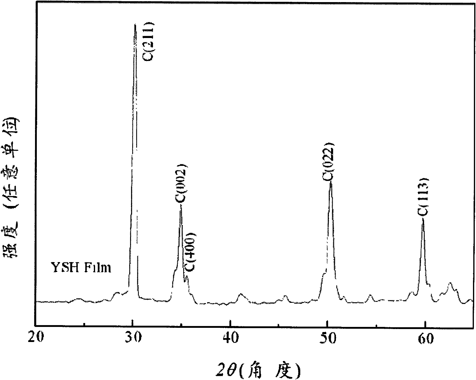
[0035] In the present invention, under high vacuum and low oxygen partial pressure conditions, an ultra-thin film with a thickness of about 5nm is made on a silicon substrate. The film is amorphous, and its dielectric constant varies with Y 2 o 3 There will be a small change in the amount of doping.

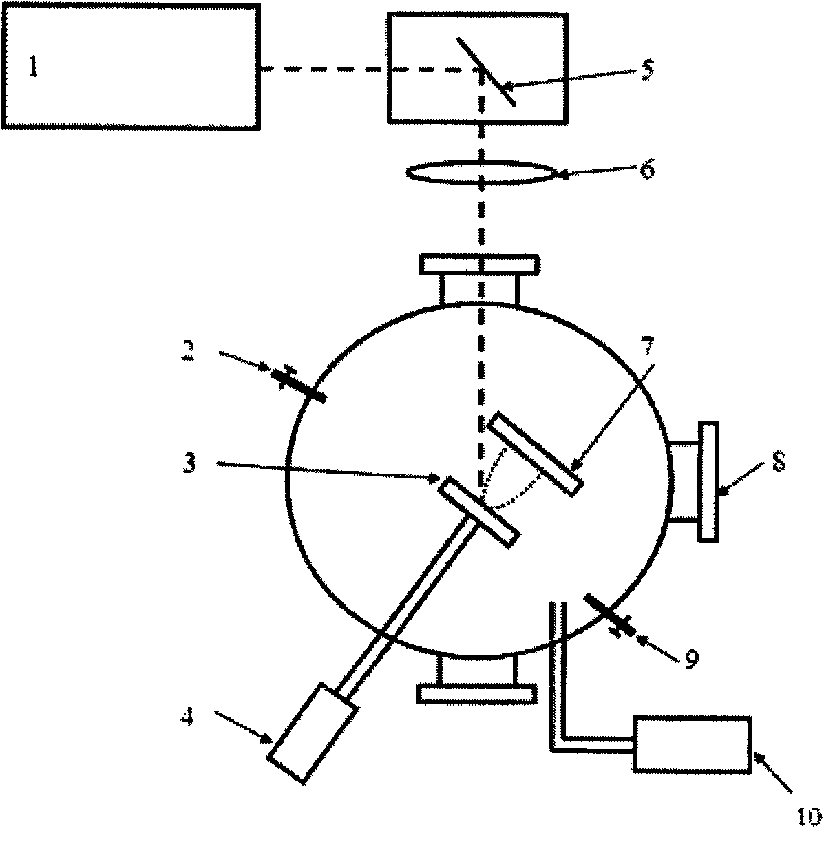
[0036] Such as figure 1 , the growth system of the present invention uses a pulsed laser deposition system, such as figure 1 , including excimer laser 1; inlet valve 2; target 3; motor 4; mirror 5; focusing lens 6; substrate table 7; observation port 8; air release valve 9; mechanical pump and molecular pump 10, pulse laser The deposition system is a prior art and will not be described in detail.

[0037] to prepare Y 2 o 3 Take a YSH film with a molar ratio of 6% as an example, and its preparation steps are as follows:

[0038] (1) Preparation of YSH ceramic target: pure Y 2 o 3 and HfO 2 The powder is mixed according to the molar ratio of 6:94, fully milled by a ball m...


PUM


Abstract

The invention relates to a gate dielectric material cubical phase HfO2 film and a preparation method thereof. A stable cubical phase HfO2 film is obtained by doping Y2O3, and the molar percentage of the doping amount of the Y2O3 is between 0 and 28. The HfO2 is in a cubical phase at normal temperature, and the dielectric constant is 27.2. The gate dielectric material cubical phase HfO2 film is prepared by using the cubical phase HfO2 ceramic target material stabilized by the Y2O3 by a pulse laser deposition technique under the conditions of high vacuum and low partial pressure of oxygen. The invention uses the method of pulse laser deposition, uses the metal oxide Y2O3 and the HfO2 as raw materials and uses the binary phase diagram of the two materials as a basis to obtain the cubical phase HfO2 which is stable at normal temperature by the high-temperature solid phase reaction at normal temperature, thereby remarkably improving the dielectric constant of the HfO2 at normal temperatureand preparing and obtaining a YSH film, the EOT value of which is less than 1.5 nm. The invention provides new vitality for the application of the HfO2 which is the most potential gate dielectric material in the future.

Description

technical field [0001] The invention belongs to the field of microelectronic materials, in particular to hafnium oxide HfO, a high dielectric constant gate dielectric material used in metal-oxide-semiconductor field effect transistor MOSFETs 2 Thin film, a gate dielectric material cubic phase HfO 2 Thin films and methods for their preparation. Background technique [0002] In 1947, Bardeen, Brattain, and Shockley invented solid-state components to replace electronic vacuum tubes, which marked the emergence of the microelectronics industry. Since the birth of solid components, the microelectronics industry has experienced four decades of unprecedented explosive growth, driven by two factors - the planar integrated circuits invented by Noyce and Kilby and the excellent performance of solid components due to scale reduction (size shrinkage). performance. Scaling down solid state components offers the rare combination of reduced cost, improved performance and power that gives...

Claims


Application Information

Patent Timeline
IPC IPC(8): C23C14/28C23C14/06
Inventor 石磊周越刘治国殷江
Owner NANJING UNIV
Why Eureka
Try Eureka