Method for manufacturing transistor by using silicon single crystal slices

A transistor and silicon single crystal technology, which is applied in the field of lightly doped/heavily doped structure silicon substrate manufacturing, can solve problems such as crystal defects, difficult operation, and stress, and achieve the effect of reducing defects and improving device performance

Active Publication Date: 2010-03-03
ZHEJIANG HAINA SEMICON CO LTD
View PDF1 Cites 7 Cited by
  • Summary
  • Abstract
  • Description
  • Claims
  • Application Information

AI Technical Summary

Problems solved by technology

But this method has the following disadvantages: 1. Due to the bonding with glass powder, there will inevitably be many bubbles at the bonding interface. The existence of bubbles will cause a large amount of stress between the two silicon wafers. In the subsequent device process , the stress will induce crystal defects

Method used


Image

  • Method for manufacturing transistor by using silicon single crystal slices
  • Method for manufacturing transistor by using silicon single crystal slices
  • Method for manufacturing transistor by using silicon single crystal slices

Examples


Embodiment 1

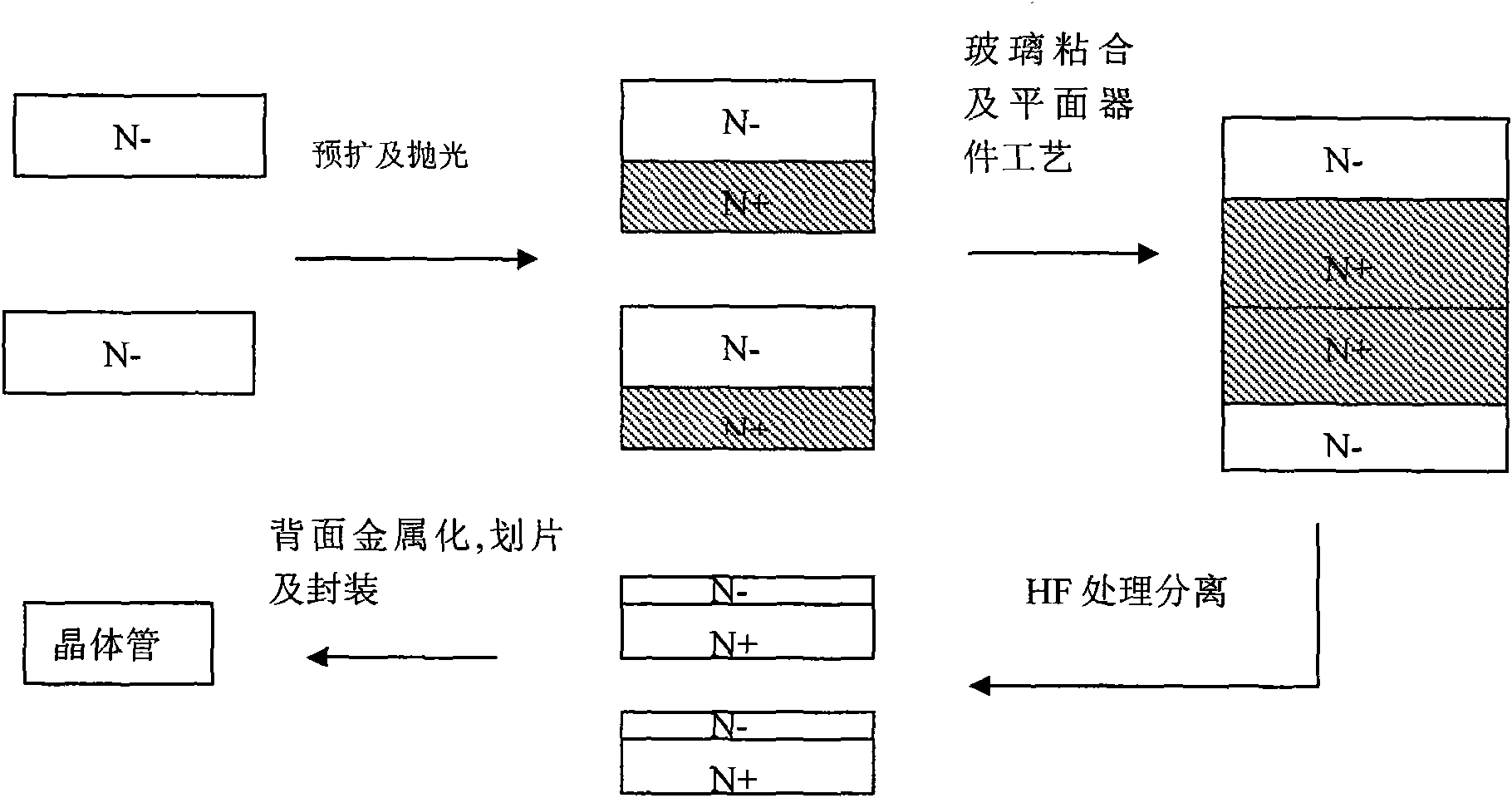
[0033] Embodiment 1, image 3 A method for bonding and separating silicon wafers is provided, and the following steps are performed in sequence:

[0034] 1) Choose 2 pieces of single crystal polished silicon wafers, the crystal orientation of the single crystal silicon wafers is , the doping type is N type, the dopant is phosphorus, and the resistivity is 33 ohm.cm to 35 ohm.cm , the front side of the single crystal polished silicon wafer is a polished surface with a surface roughness of 0.5nm, the thickness of the single crystal silicon wafer is 230um, and the diameter is 100mm.

[0035] 2), each silicon wafer is carried out as follows:

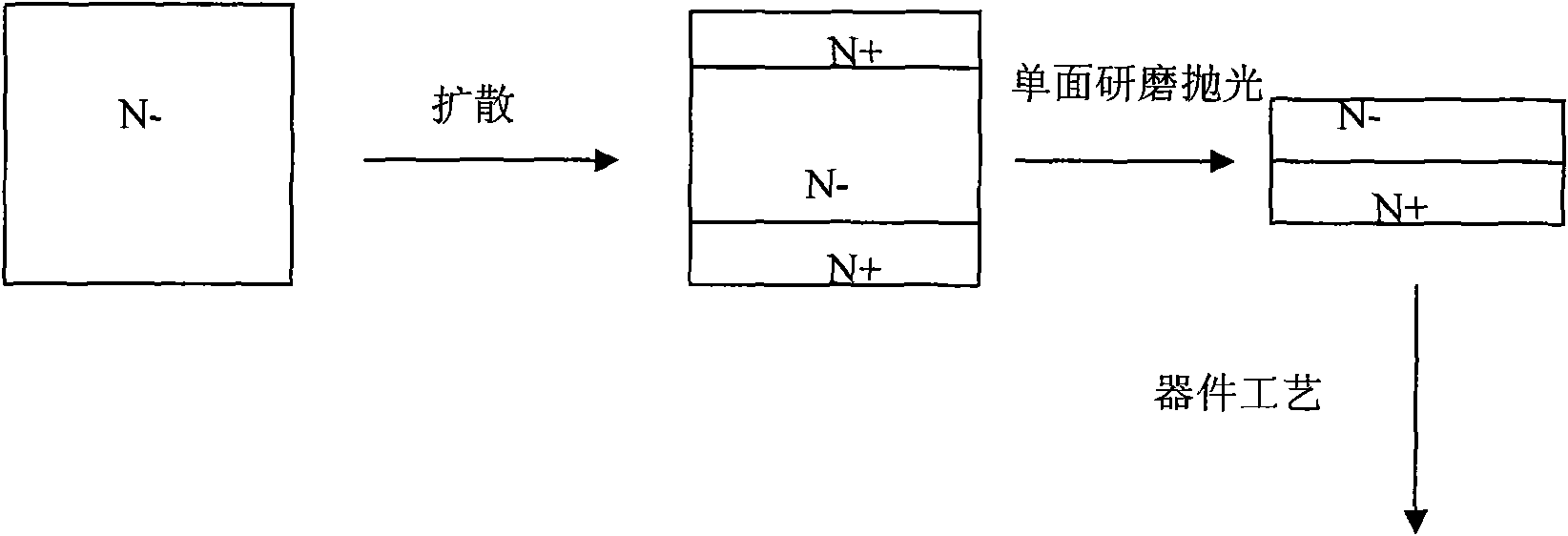
[0036] Place the silicon wafer in a high-temperature diffusion furnace, adopt a conventional phosphorus pre-expansion process, and pass a phosphorus source (POCL 3 ), and do impurity (N+) on the surface of the silicon wafer for pre-deposition and diffusion for 4 hours.

[0037] Then adopt the conventional thermal oxidation method, the pro...

Embodiment 2

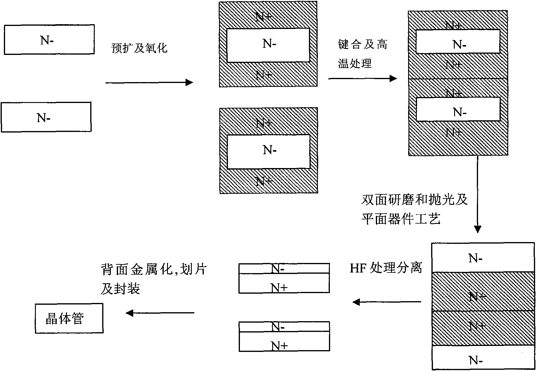
[0052] Embodiment 2, a method for bonding and separating silicon wafers, the following steps are carried out successively:

[0053] 1) Choose 2 pieces of single crystal polished silicon wafers, the crystal orientation of the single crystal silicon wafers is , the doping type is N type, the dopant is phosphorus, and the resistivity is 33 ohm.cm to 35 ohm.cm , the front side of the single crystal silicon wafer is a polished surface with a surface roughness of 0.5nm, the thickness of the single crystal silicon wafer is 170um, and the diameter is 125mm.

[0054] 2), with embodiment 1.

[0055] 3) Put the above-mentioned polished silicon wafers with an oxide layer that meet the requirements in pairs, and then perform room temperature bonding on the bonding machine. The bonding method adopts the conventional silicon wafer room temperature direct bonding method, and the air in the bonding area is clean The grade is 10, and the bonded silicon wafer group is obtained.

[0056] Then p...


PUM

PropertyMeasurementUnit
Thicknessaaaaaaaaaa
Surface roughnessaaaaaaaaaa
Thicknessaaaaaaaaaa

Abstract

The invention discloses a method for manufacturing a transistor by using silicon single crystal slices, which comprises the steps of: 1) selecting two light-doped polished silicon slices, wherein thefront surfaces thereof are the polished surfaces; 2) conducting N+ or P+ pre-expansion on each silicon slice and then arranging an oxide layer on the front surface of the pre-expanded polished siliconslice; 3) causing the front surfaces of the two polished silicon slices with the oxide layers to face to each other for bonding at room temperature, and putting the obtained bonded silicon slice group into a high-temperature furnace for high-temperature processing; 4) conducting mechanical grinding and polishing on the two surfaces of the obtained silicon slice group; 5) manufacturing a transistor chip on the two surfaces of the silicon slice group respectively; 6) putting the silicon slice group obtained in the Step 5) into an HF solution to separate the silicon slices; and 7) metallizing the surfaces of the silicon slices without the transistor chip, and then removing optical resist, scribing and packaging, thus obtaining the transistor. The method for manufacturing the transistor by using silicon single crystal slices can guarantee the performance of the transistor.

Description

technical field [0001] The invention relates to a method for manufacturing a transistor with a thin single crystal silicon wafer, mainly a method for manufacturing a lightly doped (top layer of the silicon wafer) / heavily doped (bottom layer of the silicon wafer) structure silicon substrate. Background technique [0002] There are usually two methods to produce silicon wafers with N- / N+, P / N+, N / P+, and P / P+ structures: the first method is to epitaxially layer a layer of lightly doped silicon on the surface of heavily doped silicon wafers; the second method is to use Lightly doped silicon wafers are thermally diffused in a diffusion furnace to form heavy doping on the surface, and then one side of the silicon wafers is ground and polished to achieve the above structure. Method 1, that is, the silicon wafer with the above structure made by the epitaxial method is of good quality, but the processing cost is high, and the equipment cost of the epitaxial furnace used is also high...

Claims


Application Information

Patent Timeline
IPC IPC(8): H01L21/331H01L21/02
Inventor 肖型奎
Owner ZHEJIANG HAINA SEMICON CO LTD
Why Eureka
Try Eureka