Preparation method of insulating metal substrate for high-power LED packaging
A technology of LED packaging and insulating metal, applied in semiconductor/solid-state device manufacturing, electrical components, circuits, etc., can solve problems such as affecting the thermal conductivity of insulating layers
- Summary
- Abstract
- Description
- Claims
- Application Information
AI Technical Summary
Problems solved by technology
Method used
Image
Examples
Embodiment 1
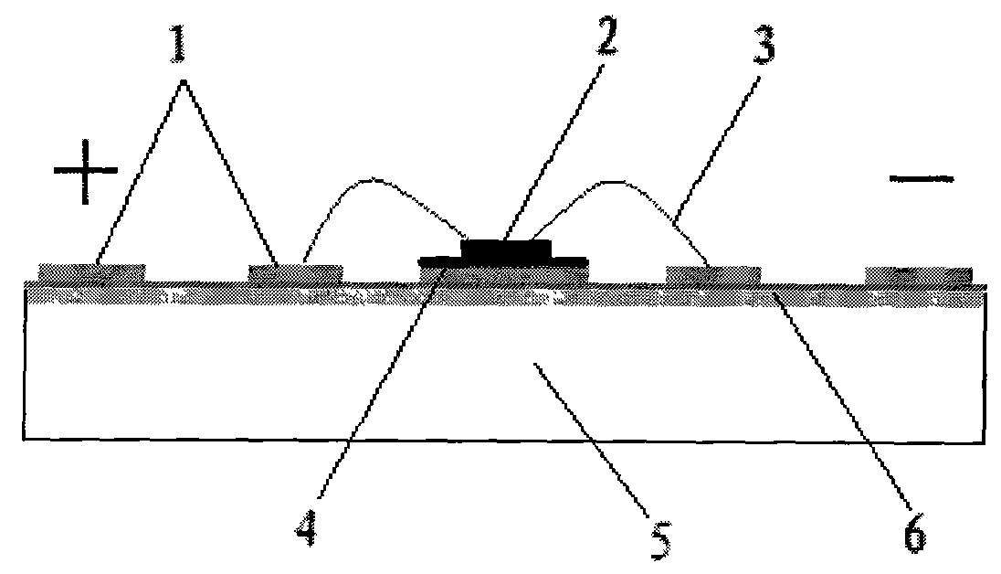
[0014] With aluminum alloy as the base material of the insulated metal substrate, generally choose an aluminum plate with high thermal conductivity and certain mechanical strength, and can withstand a certain temperature, such as 6165, 6061, 6055, 6063 and other grades of aluminum plate. The polymer precursor slurry used to prepare the insulating layer is an organosilicon precursor resin containing ceramic fillers such as aluminum nitride and silicon carbide, wherein the particle size of the ceramic powder is nanometer and submicron. The conductive layer material is copper. When used as a high-power LED packaging substrate, a layer of silver-tin eutectic solder can also be plated on the LED chip welding area.
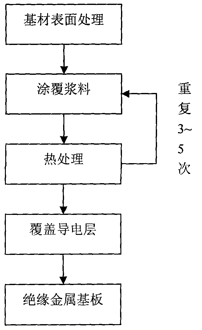
[0015] 1. First use mechanical methods to remove the oil and impurities on the surface of the aluminum plate, and then use the micro-arc oxidation process to grow a thin layer of alumina ceramics on the surface, about 5-10 μm, and then use ultrasonic cleaning to remove ...
Embodiment 2
[0019] Industrial pure copper with high thermal conductivity is selected as the base material of the insulating metal substrate, and the polymer precursor slurry used in the preparation of the insulating layer is an organosilicon precursor resin containing ceramic fillers such as silicon carbide and boron carbide. The particle size of the ceramic powder is The grades are nanoscale and submicron. The conductive layer material is copper. When used as a high-power LED packaging substrate, a layer of silver-tin eutectic solder can also be plated on the LED chip welding area.
[0020] 1. First use mechanical methods to remove oil and impurities on the surface of the copper plate, and then use sandblasting process on the surface of the copper plate to produce uniform and fine concave-convex surface on the surface of the workpiece, which enhances the adhesion between it and the coating. Then use micro-oxidation technology to produce a small amount of cuprous oxide on the surface;
...
PUM
| Property | Measurement | Unit |
|---|---|---|
| Thickness | aaaaa | aaaaa |
Abstract
Description
Claims
Application Information


